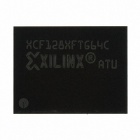
XCF128XFTG64C Xilinx Inc, XCF128XFTG64C Datasheet - Page 54

XCF128XFTG64C
Manufacturer Part Number
XCF128XFTG64C
Description
IC PROM SRL 128M GATE 64-FTBGA
Manufacturer
Xilinx Inc
Datasheet
1.XCF128XFTG64C.pdf
(88 pages)
Specifications of XCF128XFTG64C
Memory Size
128Mb
Programmable Type
In System Programmable
Voltage - Supply
1.7 V ~ 2 V
Operating Temperature
-40°C ~ 85°C
Package / Case
64-TBGA
Access Time
85ns
Supply Voltage Range
1.7V To 2V
Memory Case Style
FTBGA
No. Of Pins
64
Operating Temperature Range
-40°C To +85°C
Svhc
No SVHC (15-Dec-2010)
Package /
RoHS Compliant
Lead Free Status / RoHS Status
Lead free / RoHS Compliant
Other names
122-1578
Available stocks
Company
Part Number
Manufacturer
Quantity
Price
Company:
Part Number:
XCF128XFTG64C
Manufacturer:
XILINX
Quantity:
319
Part Number:
XCF128XFTG64C
Manufacturer:
XILINX/赛灵思
Quantity:
20 000
Table 30: Write AC Characteristics, Write Enable Controlled
Notes:
1.
2.
3.
DS617 (v3.0.1) January 07, 2010
Product Specification
Sampled only, not 100% tested.
Meaningful only if L is always kept Low.
T
System designers should take this timing into account and can insert a software No-Op instruction to delay the first read in the same bank after
issuing any command and to delay the first read to any address after issuing a Set Configuration Register command. If the first read after the
command is a Read Array operation in a different bank and no changes to the Configuration Register are issued, T
Symbol
WHEL
T
T
T
T
T
T
T
T
T
T
T
T
T
T
T
T
T
T
T
T
T
T
T
T
T
T
AVAV
AVLH
AVWH
DVWH
ELLH
ELWL
ELQV
ELKV
GHWL
LHAX
LLLH
WHAV
WHAX
WHDX
WHEH
WHEL
WHGL
WHLL
WHWL
WLWH
QVVPL
QVWPL
VPHWH
WHVPL
WHWPL
WPHWH
and T
R
(3)
(2)
(2)
(3)
(2)
WHLL
T
T
T
T
T
T
T
T
T
Alt
WPH
VPS
have this value when reading in the targeted bank or when reading following a Set Configuration Register command.
WC
WP
AH
DH
CH
DS
CS
Address Valid to Next Address Valid
Address Valid to Latch Enable High
Address Valid to Write Enable High
Data Valid to Write Enable High
Chip Enable Low to Latch Enable High
Chip Enable Low to Write Enable Low
Chip Enable Low to Output Valid
Chip Enable Low to Clock Valid
Output Enable High to Write Enable Low
Latch Enable High to Address Transition
Latch Enable Pulse Width
Write Enable High to Address Valid
Write Enable High to Address Transition
Write Enable High to Input Transition
Write Enable High to Chip Enable High
Write Enable High to Chip Enable Low
Write Enable High to Output Enable Low
Write Enable High to Latch Enable Low
Write Enable High to Write Enable Low
Write Enable Low to Write Enable High
Output (Status Register) Valid to V
Output (Status Register) Valid to Write Protect Low
V
Write Enable High to V
Write Enable High to Write Protect Low
Write Protect High to Write Enable High
PP
High to Write Enable High
PP
Parameter
Low
Platform Flash XL High-Density Configuration and Storage Device
www.xilinx.com
PP
Low
(1)
Min
Min
Min
Min
Min
Min
Min
Min
Min
Min
Min
Min
Min
Min
Min
Min
Min
Min
Min
Min
Min
Min
Min
Min
Min
Min
2.3V to 2.7V
V
DDQ
200
200
200
200
85
10
50
10
85
17
10
25
25
25
50
50
9
0
0
0
0
0
0
9
0
0
Voltage Range
=
3.0V to 3.6V
WHEL
V
DDQ
200
200
200
200
85
10
50
50
10
85
17
10
25
25
25
50
and T
0
9
9
0
0
0
0
0
0
0
=
WHLL
are 0 ns.
Unit
ns
ns
ns
ns
ns
ns
ns
ns
ns
ns
ns
ns
ns
ns
ns
ns
ns
ns
ns
ns
ns
ns
ns
ns
ns
ns
54


