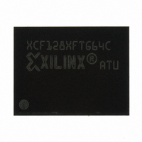
XCF128XFTG64C Xilinx Inc, XCF128XFTG64C Datasheet - Page 67

XCF128XFTG64C
Manufacturer Part Number
XCF128XFTG64C
Description
IC PROM SRL 128M GATE 64-FTBGA
Manufacturer
Xilinx Inc
Datasheet
1.XCF128XFTG64C.pdf
(88 pages)
Specifications of XCF128XFTG64C
Memory Size
128Mb
Programmable Type
In System Programmable
Voltage - Supply
1.7 V ~ 2 V
Operating Temperature
-40°C ~ 85°C
Package / Case
64-TBGA
Access Time
85ns
Supply Voltage Range
1.7V To 2V
Memory Case Style
FTBGA
No. Of Pins
64
Operating Temperature Range
-40°C To +85°C
Svhc
No SVHC (15-Dec-2010)
Package /
RoHS Compliant
Lead Free Status / RoHS Status
Lead free / RoHS Compliant
Other names
122-1578
Available stocks
Company
Part Number
Manufacturer
Quantity
Price
Company:
Part Number:
XCF128XFTG64C
Manufacturer:
XILINX
Quantity:
319
Part Number:
XCF128XFTG64C
Manufacturer:
XILINX/赛灵思
Quantity:
20 000
Table 44: Bank and Erase Block Region 1 Information
DS617 (v3.0.1) January 07, 2010
Product Specification
Notes:
1.
2.
The variable P is a pointer which is defined at CFI offset 015h.
Bank Regions. There are two Bank Regions, see
(P+2A)h = 134h
(P+2B)h = 135h
(P+2C)h = 136h
(P+2D)h = 137h
(P+2E)h = 138h
(P+2F)h = 139h
(P+24)h = 12Eh
(P+25)h = 12Fh
(P+26)h = 130h
(P+27)h = 131h
(P+28)h = 132h
(P+29)h = 133h
(P+30)h = 13Ah
(P+31)h = 13Bh
Offset
–
R
Data
0Fh
00h
11h
00h
00h
01h
07h
00h
00h
02h
64h
00h
01h
03h
–
Number of identical banks within Bank Region 1
Number of program or erase operations allowed in Bank Region 1:
Number of program or erase operations allowed in other banks while a bank in same region is
programming
Number of program or erase operations allowed in other banks while a bank in this region is
erasing
Types of erase block regions in Bank Region 1 n = number of erase block regions with
contiguous same-sized erase blocks. Symmetrically blocked banks have one blocking
region
Bank Region 1 Erase Block Type 1 Information:
Bank Region 1 (Erase Block Type 1)
Minimum block erase cycles × 1000
Bank Region 1 (Erase Block Type 1): BIts per cell, internal ECC
Bank Region 1 (Erase Block Type 1): Page mode and Synchronous mode capabilities
Bank Region 1 Erase Block Type 2 Information
Bank Region 1 (Erase Block Type 2)
Minimum block erase cycles × 1000
Bank Regions 1 (Erase Block Type 2): Bits per cell, internal ECC
Bank Region 1 (Erase Block Type 2): Page mode and Synchronous mode capabilities
Bits 0–3: Number of simultaneous program operations Bits
4–7: Number of simultaneous erase operations
Bits 0–3: Number of simultaneous program operations
Bits 4–7: Number of simultaneous erase operations
Bits 0–3: Number of simultaneous program operations Bits
4–7: Number of simultaneous erase operations
Bits 0–15: n+1 = number of identical-sized erase blocks
Bits 16–31: n×256 = number of bytes in erase block region
Bits 0–3: bits per cell in erase region
Bit 4: reserved for “internal ECC used”
BIts 5–7: reserved
Bit 0: Page-mode reads permitted
Bit 1: Synchronous reads permitted
Bit 2: Synchronous writes permitted
Bits 3–7: reserved
Bits 0–15: n+1 = number of identical-sized erase blocks
Bits 16–31: n×256 = number of bytes in erase block region
Bits 0–3: bits per cell in erase region
Bit 4: reserved for “internal ECC used”
Bits 5–7: reserved
Bit 0: Page-mode reads permitted
Bit 1: Synchronous reads permitted
Bit 2: Synchronous writes permitted
Bits 3–7: reserved
(2)
.
Table 35, page
Platform Flash XL High-Density Configuration and Storage Device
www.xilinx.com
(1,2)
61.
Description
67


