C8051F040DK Silicon Laboratories Inc, C8051F040DK Datasheet - Page 12
C8051F040DK
Manufacturer Part Number
C8051F040DK
Description
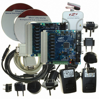
DEV KIT FOR F040/F041/F042/F043
Manufacturer
Silicon Laboratories Inc
Type
MCUr
Specifications of C8051F040DK
Contents
Evaluation Board, Power Supply, USB Cables, Adapter and Documentation
Processor To Be Evaluated
C8051F04x
Interface Type
USB
Silicon Manufacturer
Silicon Labs
Core Architecture
8051
Silicon Core Number
C8051F040
Silicon Family Name
C8051F04x
Lead Free Status / RoHS Status
Contains lead / RoHS non-compliant
For Use With/related Products
Silicon Laboratories C8051 F040, 041, 042, 043 MCUs
Lead Free Status / Rohs Status
Lead free / RoHS Compliant
Other names
336-1205
Available stocks
Company
Part Number
Manufacturer
Quantity
Price
Company:

Part Number:
C8051F040DK
Manufacturer:
SiliconL
Quantity:
9


C8051F040/1/2/3/4/5/6/7
22. UART1
23. Timers
24. Programmable Counter Array
25. JTAG (IEEE 1149.1)
12
Figure 22.1. UART1 Block Diagram ....................................................................... 277
Figure 22.2. UART1 Baud Rate Logic .................................................................... 278
Figure 22.3. UART Interconnect Diagram .............................................................. 279
Figure 22.4. 8-Bit UART Timing Diagram............................................................... 279
Figure 22.5. 9-Bit UART Timing Diagram............................................................... 280
Figure 22.6. UART Multi-Processor Mode Interconnect Diagram .......................... 281
Figure 23.1. T0 Mode 0 Block Diagram.................................................................. 288
Figure 23.2. T0 Mode 2 Block Diagram.................................................................. 289
Figure 23.3. T0 Mode 3 Block Diagram.................................................................. 290
Figure 23.4. Tn Capture Mode Block Diagram ....................................................... 296
Figure 23.5. Tn Auto-reload Mode and Toggle Mode Block Diagram .................... 297
Figure 24.1. PCA Block Diagram............................................................................ 303
Figure 24.2. PCA Counter/Timer Block Diagram.................................................... 304
Figure 24.3. PCA Interrupt Block Diagram ............................................................. 305
Figure 24.4. PCA Capture Mode Diagram.............................................................. 306
Figure 24.5. PCA Software Timer Mode Diagram .................................................. 307
Figure 24.6. PCA High-Speed Output Mode Diagram............................................ 308
Figure 24.7. PCA Frequency Output Mode ............................................................ 309
Figure 24.8. PCA 8-Bit PWM Mode Diagram ......................................................... 310
Figure 24.9. PCA 16-Bit PWM Mode...................................................................... 311
Rev. 1.5
Related parts for C8051F040DK
Image
Part Number
Description
Manufacturer
Datasheet
Request
R

Part Number:
Description:
SMD/C°/SINGLE-ENDED OUTPUT SILICON OSCILLATOR
Manufacturer:
Silicon Laboratories Inc
Part Number:
Description:
Manufacturer:
Silicon Laboratories Inc
Datasheet:
Part Number:
Description:
N/A N/A/SI4010 AES KEYFOB DEMO WITH LCD RX
Manufacturer:
Silicon Laboratories Inc
Datasheet:
Part Number:
Description:
N/A N/A/SI4010 SIMPLIFIED KEY FOB DEMO WITH LED RX
Manufacturer:
Silicon Laboratories Inc
Datasheet:
Part Number:
Description:
N/A/-40 TO 85 OC/EZLINK MODULE; F930/4432 HIGH BAND (REV E/B1)
Manufacturer:
Silicon Laboratories Inc
Part Number:
Description:
EZLink Module; F930/4432 Low Band (rev e/B1)
Manufacturer:
Silicon Laboratories Inc
Part Number:
Description:
I°/4460 10 DBM RADIO TEST CARD 434 MHZ
Manufacturer:
Silicon Laboratories Inc
Part Number:
Description:
I°/4461 14 DBM RADIO TEST CARD 868 MHZ
Manufacturer:
Silicon Laboratories Inc
Part Number:
Description:
I°/4463 20 DBM RFSWITCH RADIO TEST CARD 460 MHZ
Manufacturer:
Silicon Laboratories Inc
Part Number:
Description:
I°/4463 20 DBM RADIO TEST CARD 868 MHZ
Manufacturer:
Silicon Laboratories Inc
Part Number:
Description:
I°/4463 27 DBM RADIO TEST CARD 868 MHZ
Manufacturer:
Silicon Laboratories Inc
Part Number:
Description:
I°/4463 SKYWORKS 30 DBM RADIO TEST CARD 915 MHZ
Manufacturer:
Silicon Laboratories Inc
Part Number:
Description:
N/A N/A/-40 TO 85 OC/4463 RFMD 30 DBM RADIO TEST CARD 915 MHZ
Manufacturer:
Silicon Laboratories Inc
Part Number:
Description:
I°/4463 20 DBM RADIO TEST CARD 169 MHZ
Manufacturer:
Silicon Laboratories Inc