C8051F040DK Silicon Laboratories Inc, C8051F040DK Datasheet - Page 203
C8051F040DK
Manufacturer Part Number
C8051F040DK
Description
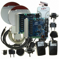
DEV KIT FOR F040/F041/F042/F043
Manufacturer
Silicon Laboratories Inc
Type
MCUr
Specifications of C8051F040DK
Contents
Evaluation Board, Power Supply, USB Cables, Adapter and Documentation
Processor To Be Evaluated
C8051F04x
Interface Type
USB
Silicon Manufacturer
Silicon Labs
Core Architecture
8051
Silicon Core Number
C8051F040
Silicon Family Name
C8051F04x
Lead Free Status / RoHS Status
Contains lead / RoHS non-compliant
For Use With/related Products
Silicon Laboratories C8051 F040, 041, 042, 043 MCUs
Lead Free Status / Rohs Status
Lead free / RoHS Compliant
Other names
336-1205
Available stocks
Company
Part Number
Manufacturer
Quantity
Price
Company:

Part Number:
C8051F040DK
Manufacturer:
SiliconL
Quantity:
9


17. Port Input/Output
The C8051F04x family of devices are fully integrated mixed-signal System on a Chip MCUs with 64 digital
I/O pins (C8051F040/2/4/6) or 32 digital I/O pins (C8051F041/3/5/7), organized as 8-bit Ports. All ports are
both bit- and byte-addressable through their corresponding Port Data registers. All Port pins are 5 V-toler-
ant, and all support configurable Open-Drain or Push-Pull output modes and weak pullups. A block dia-
gram of the Port I/O cell is shown in Figure 17.1. Complete Electrical Specifications for the Port I/O pins
are given in Table 17.1.
Table 17.1. Port I/O DC Electrical Characteristics
V
Output High Voltage
(V
Output Low Voltage
(V
Input High Voltage (VIH)
Input Low Voltage (VIL)
Input Leakage Current
Input Capacitance
DD
OH
OL
PORT-INPUT
/WEAK-PULLUP
PUSH-PULL
/PORT-OUTENABLE
PORT-OUTPUT
ANALOG INPUT
= 2.7 to 3.6 V, –40 to +85 °C unless otherwise specified.
)
)
Parameter
Analog Select
(Ports 1, 2, and 3)
I
I
I
I
I
I
DGND < Port Pin < V
Weak Pullup Off
Weak Pullup On
OH
OH
OH
OL
OL
OL
Figure 17.1. Port I/O Cell Block Diagram
= 8.5 mA
= 10 µA
= 25 mA
= –3 mA, Port I/O Push-Pull
= –10 µA, Port I/O Push-Pull
= –10 mA, Port I/O Push-Pull
Conditions
DD
Rev. 1.5
, Pin Tri-state
C8051F040/1/2/3/4/5/6/7
DGND
V
V
0.7 x V
VDD
DD
DD
Min
—
—
—
—
—
—
—
—
—
– 0.7
– 0.1
DD
V
DD
VDD
Typ
1.0
10
—
—
—
—
—
—
—
—
5
(WEAK)
– 0.8
0.3 x V
Max
0.6
0.1
± 1
—
—
—
—
—
—
—
—
DD
PORT
PAD
Units
µA
pF
V
V
203
Related parts for C8051F040DK
Image
Part Number
Description
Manufacturer
Datasheet
Request
R

Part Number:
Description:
SMD/C°/SINGLE-ENDED OUTPUT SILICON OSCILLATOR
Manufacturer:
Silicon Laboratories Inc
Part Number:
Description:
Manufacturer:
Silicon Laboratories Inc
Datasheet:
Part Number:
Description:
N/A N/A/SI4010 AES KEYFOB DEMO WITH LCD RX
Manufacturer:
Silicon Laboratories Inc
Datasheet:
Part Number:
Description:
N/A N/A/SI4010 SIMPLIFIED KEY FOB DEMO WITH LED RX
Manufacturer:
Silicon Laboratories Inc
Datasheet:
Part Number:
Description:
N/A/-40 TO 85 OC/EZLINK MODULE; F930/4432 HIGH BAND (REV E/B1)
Manufacturer:
Silicon Laboratories Inc
Part Number:
Description:
EZLink Module; F930/4432 Low Band (rev e/B1)
Manufacturer:
Silicon Laboratories Inc
Part Number:
Description:
I°/4460 10 DBM RADIO TEST CARD 434 MHZ
Manufacturer:
Silicon Laboratories Inc
Part Number:
Description:
I°/4461 14 DBM RADIO TEST CARD 868 MHZ
Manufacturer:
Silicon Laboratories Inc
Part Number:
Description:
I°/4463 20 DBM RFSWITCH RADIO TEST CARD 460 MHZ
Manufacturer:
Silicon Laboratories Inc
Part Number:
Description:
I°/4463 20 DBM RADIO TEST CARD 868 MHZ
Manufacturer:
Silicon Laboratories Inc
Part Number:
Description:
I°/4463 27 DBM RADIO TEST CARD 868 MHZ
Manufacturer:
Silicon Laboratories Inc
Part Number:
Description:
I°/4463 SKYWORKS 30 DBM RADIO TEST CARD 915 MHZ
Manufacturer:
Silicon Laboratories Inc
Part Number:
Description:
N/A N/A/-40 TO 85 OC/4463 RFMD 30 DBM RADIO TEST CARD 915 MHZ
Manufacturer:
Silicon Laboratories Inc
Part Number:
Description:
I°/4463 20 DBM RADIO TEST CARD 169 MHZ
Manufacturer:
Silicon Laboratories Inc