C8051F040DK Silicon Laboratories Inc, C8051F040DK Datasheet - Page 5
C8051F040DK
Manufacturer Part Number
C8051F040DK
Description
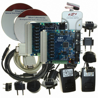
DEV KIT FOR F040/F041/F042/F043
Manufacturer
Silicon Laboratories Inc
Type
MCUr
Specifications of C8051F040DK
Contents
Evaluation Board, Power Supply, USB Cables, Adapter and Documentation
Processor To Be Evaluated
C8051F04x
Interface Type
USB
Silicon Manufacturer
Silicon Labs
Core Architecture
8051
Silicon Core Number
C8051F040
Silicon Family Name
C8051F04x
Lead Free Status / RoHS Status
Contains lead / RoHS non-compliant
For Use With/related Products
Silicon Laboratories C8051 F040, 041, 042, 043 MCUs
Lead Free Status / Rohs Status
Lead free / RoHS Compliant
Other names
336-1205
Available stocks
Company
Part Number
Manufacturer
Quantity
Price
Company:

Part Number:
C8051F040DK
Manufacturer:
SiliconL
Quantity:
9


15. Flash Memory ....................................................................................................... 179
16. External Data Memory Interface and On-Chip XRAM........................................ 187
17. Port Input/Output.................................................................................................. 203
18. Controller Area Network (CAN0) ......................................................................... 227
14.2.External Oscillator Drive Circuit...................................................................... 175
14.3.System Clock Selection.................................................................................. 175
14.4.External Crystal Example ............................................................................... 177
14.5.External RC Example ..................................................................................... 178
14.6.External Capacitor Example ........................................................................... 178
15.1.Programming The Flash Memory ................................................................... 179
15.2.Non-volatile Data Storage .............................................................................. 180
15.3.Security Options ............................................................................................. 180
16.1.Accessing XRAM............................................................................................ 187
16.2.Configuring the External Memory Interface .................................................... 188
16.3.Port Selection and Configuration.................................................................... 188
16.4.Multiplexed and Non-multiplexed Selection.................................................... 191
16.5.Memory Mode Selection................................................................................. 193
16.6.Timing .......................................................................................................... 194
17.1.Ports 0 through 3 and the Priority Crossbar Decoder..................................... 204
17.2.Ports 4 through 7 ............................................................................................ 220
18.1.Bosch CAN Controller Operation.................................................................... 228
15.3.1.Summary of Flash Security Options....................................................... 183
16.1.1.16-Bit MOVX Example ........................................................................... 187
16.1.2.8-Bit MOVX Example ............................................................................. 187
16.4.1.Multiplexed Configuration....................................................................... 191
16.4.2.Non-multiplexed Configuration............................................................... 192
16.5.1.Internal XRAM Only ............................................................................... 193
16.5.2.Split Mode without Bank Select.............................................................. 193
16.5.3.Split Mode with Bank Select................................................................... 194
16.5.4.External Only.......................................................................................... 194
16.6.1.Non-multiplexed Mode ........................................................................... 196
16.6.2.Multiplexed Mode ................................................................................... 199
17.1.1.Crossbar Pin Assignment and Allocation ............................................... 205
17.1.2.Configuring the Output Modes of the Port Pins...................................... 206
17.1.3.Configuring Port Pins as Digital Inputs................................................... 206
17.1.4.Weak Pullups ......................................................................................... 207
17.1.5.Configuring Port 1, 2, and 3 Pins as Analog Inputs ............................... 207
17.1.6.External Memory Interface Pin Assignments ......................................... 208
17.1.7.Crossbar Pin Assignment Example........................................................ 210
17.2.1.Configuring Ports Which are Not Pinned Out......................................... 221
17.2.2.Configuring the Output Modes of the Port Pins...................................... 221
17.2.3.Configuring Port Pins as Digital Inputs................................................... 221
17.2.4.Weak Pullups ......................................................................................... 221
17.2.5.External Memory Interface ..................................................................... 221
18.1.1.CAN Controller Timing ........................................................................... 229
Rev. 1.5
C8051F040/1/2/3/4/5/6/7
5
Related parts for C8051F040DK
Image
Part Number
Description
Manufacturer
Datasheet
Request
R

Part Number:
Description:
SMD/C°/SINGLE-ENDED OUTPUT SILICON OSCILLATOR
Manufacturer:
Silicon Laboratories Inc
Part Number:
Description:
Manufacturer:
Silicon Laboratories Inc
Datasheet:
Part Number:
Description:
N/A N/A/SI4010 AES KEYFOB DEMO WITH LCD RX
Manufacturer:
Silicon Laboratories Inc
Datasheet:
Part Number:
Description:
N/A N/A/SI4010 SIMPLIFIED KEY FOB DEMO WITH LED RX
Manufacturer:
Silicon Laboratories Inc
Datasheet:
Part Number:
Description:
N/A/-40 TO 85 OC/EZLINK MODULE; F930/4432 HIGH BAND (REV E/B1)
Manufacturer:
Silicon Laboratories Inc
Part Number:
Description:
EZLink Module; F930/4432 Low Band (rev e/B1)
Manufacturer:
Silicon Laboratories Inc
Part Number:
Description:
I°/4460 10 DBM RADIO TEST CARD 434 MHZ
Manufacturer:
Silicon Laboratories Inc
Part Number:
Description:
I°/4461 14 DBM RADIO TEST CARD 868 MHZ
Manufacturer:
Silicon Laboratories Inc
Part Number:
Description:
I°/4463 20 DBM RFSWITCH RADIO TEST CARD 460 MHZ
Manufacturer:
Silicon Laboratories Inc
Part Number:
Description:
I°/4463 20 DBM RADIO TEST CARD 868 MHZ
Manufacturer:
Silicon Laboratories Inc
Part Number:
Description:
I°/4463 27 DBM RADIO TEST CARD 868 MHZ
Manufacturer:
Silicon Laboratories Inc
Part Number:
Description:
I°/4463 SKYWORKS 30 DBM RADIO TEST CARD 915 MHZ
Manufacturer:
Silicon Laboratories Inc
Part Number:
Description:
N/A N/A/-40 TO 85 OC/4463 RFMD 30 DBM RADIO TEST CARD 915 MHZ
Manufacturer:
Silicon Laboratories Inc
Part Number:
Description:
I°/4463 20 DBM RADIO TEST CARD 169 MHZ
Manufacturer:
Silicon Laboratories Inc