C8051F040DK Silicon Laboratories Inc, C8051F040DK Datasheet - Page 166
C8051F040DK
Manufacturer Part Number
C8051F040DK
Description
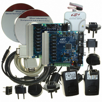
DEV KIT FOR F040/F041/F042/F043
Manufacturer
Silicon Laboratories Inc
Type
MCUr
Specifications of C8051F040DK
Contents
Evaluation Board, Power Supply, USB Cables, Adapter and Documentation
Processor To Be Evaluated
C8051F04x
Interface Type
USB
Silicon Manufacturer
Silicon Labs
Core Architecture
8051
Silicon Core Number
C8051F040
Silicon Family Name
C8051F04x
Lead Free Status / RoHS Status
Contains lead / RoHS non-compliant
For Use With/related Products
Silicon Laboratories C8051 F040, 041, 042, 043 MCUs
Lead Free Status / Rohs Status
Lead free / RoHS Compliant
Other names
336-1205
Available stocks
Company
Part Number
Manufacturer
Quantity
Price
Company:

Part Number:
C8051F040DK
Manufacturer:
SiliconL
Quantity:
9


C8051F040/1/2/3/4/5/6/7
13.1. Power-On Reset
The C8051F04x family incorporates a power supply monitor that holds the MCU in the reset state until V
rises above the V
the Electrical Characteristics of the power supply monitor circuit. The /RST pin is asserted low until the end
of the 100 ms V
enabled and disabled using the external V
On exit from a power-on reset, the PORSF flag (RSTSRC.1) is set by hardware to logic 1. All of the other
reset flags in the RSTSRC register are indeterminate. PORSF is cleared by all other resets. Since all
resets cause program execution to begin at the same location (0x0000), software can read the PORSF
flag to determine if a power-up was the cause of reset. The contents of internal data memory should be
assumed to be undefined after a power-on reset.
13.2. Power-Fail Reset
When a power-down transition or power irregularity causes V
monitor will drive the /RST pin low and return the CIP-51 to the reset state. When V
above V
Figure 13.2). Note that even though internal data memory contents are not altered by the power-fail reset,
it is impossible to determine if V
set to logic 1, the data may no longer be valid.
13.3. External Reset
The external /RST pin provides a means for external circuitry to force the MCU into a reset state. Asserting
the /RST pin low will cause the MCU to enter the reset state. It may be desirable to provide an external pul-
166
Logic HIGH
Logic LOW
RST
, the CIP-51 will leave the reset state in the same manner as that for the power-on reset (see
2.70
2.55
2.0
1.0
DD
RST
Monitor timeout in order to allow the V
/RST
level during power-up. See Figure 13.2 for timing diagram, and refer to Table 13.1 for
V
RST
DD
dropped below the level required for data retention. If the PORSF flag is
Figure 13.2. Reset Timing
Power-On Reset
DD
Reset Time
Delay
monitor enable pin (MONEN).
Rev. 1.5
DD
supply to stabilize. The V
DD
to drop below V
VDD Monitor Reset
Reset Time
Delay
RST
DD
, the power supply
DD
returns to a level
Monitor reset is
t
DD
Related parts for C8051F040DK
Image
Part Number
Description
Manufacturer
Datasheet
Request
R

Part Number:
Description:
SMD/C°/SINGLE-ENDED OUTPUT SILICON OSCILLATOR
Manufacturer:
Silicon Laboratories Inc
Part Number:
Description:
Manufacturer:
Silicon Laboratories Inc
Datasheet:
Part Number:
Description:
N/A N/A/SI4010 AES KEYFOB DEMO WITH LCD RX
Manufacturer:
Silicon Laboratories Inc
Datasheet:
Part Number:
Description:
N/A N/A/SI4010 SIMPLIFIED KEY FOB DEMO WITH LED RX
Manufacturer:
Silicon Laboratories Inc
Datasheet:
Part Number:
Description:
N/A/-40 TO 85 OC/EZLINK MODULE; F930/4432 HIGH BAND (REV E/B1)
Manufacturer:
Silicon Laboratories Inc
Part Number:
Description:
EZLink Module; F930/4432 Low Band (rev e/B1)
Manufacturer:
Silicon Laboratories Inc
Part Number:
Description:
I°/4460 10 DBM RADIO TEST CARD 434 MHZ
Manufacturer:
Silicon Laboratories Inc
Part Number:
Description:
I°/4461 14 DBM RADIO TEST CARD 868 MHZ
Manufacturer:
Silicon Laboratories Inc
Part Number:
Description:
I°/4463 20 DBM RFSWITCH RADIO TEST CARD 460 MHZ
Manufacturer:
Silicon Laboratories Inc
Part Number:
Description:
I°/4463 20 DBM RADIO TEST CARD 868 MHZ
Manufacturer:
Silicon Laboratories Inc
Part Number:
Description:
I°/4463 27 DBM RADIO TEST CARD 868 MHZ
Manufacturer:
Silicon Laboratories Inc
Part Number:
Description:
I°/4463 SKYWORKS 30 DBM RADIO TEST CARD 915 MHZ
Manufacturer:
Silicon Laboratories Inc
Part Number:
Description:
N/A N/A/-40 TO 85 OC/4463 RFMD 30 DBM RADIO TEST CARD 915 MHZ
Manufacturer:
Silicon Laboratories Inc
Part Number:
Description:
I°/4463 20 DBM RADIO TEST CARD 169 MHZ
Manufacturer:
Silicon Laboratories Inc