C8051F040DK Silicon Laboratories Inc, C8051F040DK Datasheet - Page 35
C8051F040DK
Manufacturer Part Number
C8051F040DK
Description
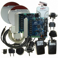
DEV KIT FOR F040/F041/F042/F043
Manufacturer
Silicon Laboratories Inc
Type
MCUr
Specifications of C8051F040DK
Contents
Evaluation Board, Power Supply, USB Cables, Adapter and Documentation
Processor To Be Evaluated
C8051F04x
Interface Type
USB
Silicon Manufacturer
Silicon Labs
Core Architecture
8051
Silicon Core Number
C8051F040
Silicon Family Name
C8051F04x
Lead Free Status / RoHS Status
Contains lead / RoHS non-compliant
For Use With/related Products
Silicon Laboratories C8051 F040, 041, 042, 043 MCUs
Lead Free Status / Rohs Status
Lead free / RoHS Compliant
Other names
336-1205
Available stocks
Company
Part Number
Manufacturer
Quantity
Price
Company:

Part Number:
C8051F040DK
Manufacturer:
SiliconL
Quantity:
9


2.
Table 2.1. Absolute Maximum Ratings*
Ambient temperature under bias
Storage Temperature
Voltage on any Pin (except V
pins) with respect to DGND
Voltage on any Port I/O Pin, /RST, and JTAG pins with
respect to DGND
Voltage on V
Maximum Total current through V
and AGND
Maximum output current sunk by any Port pin
Maximum output current sunk by any other I/O pin
Maximum output current sourced by any Port pin
Maximum output current sourced by any other I/O pin
*Note: Stresses above those listed under “Absolute Maximum Ratings” may cause permanent damage to the device.
Absolute Maximum Ratings
This is a stress rating only and functional operation of the devices at those or any other conditions above those
indicated in the operation listings of this specification is not implied. Exposure to maximum rating conditions for
extended periods may affect device reliability.
Due to special I/O design requirements of the High Voltage Difference Amplifier, undue electrical over-voltage
stress (i.e., ESD) experienced by these pads may result in impedance degradation of these inputs (HVAIN+
and HVAIN–). For this reason, care should be taken to ensure proper handling and use as typically required to
prevent ESD damage to electrostatically sensitive CMOS devices (e.g., static-free workstations, use of
grounding straps, over-voltage protection in end-applications, etc.)
DD
with respect to DGND
Parameter
DD
, Port I/O, and JTAG
DD
, AV+, DGND,
Rev. 1.5
C8051F040/1/2/3/4/5/6/7
Conditions
–0.3
–0.3
–0.3
Min
–55
–65
—
—
—
—
—
Typ
—
—
—
—
—
—
—
—
—
—
V
Max
125
150
800
100
100
DD
0.3
5.8
4.2
50
50
+
Units
mA
mA
mA
mA
mA
°C
°C
V
V
V
35
Related parts for C8051F040DK
Image
Part Number
Description
Manufacturer
Datasheet
Request
R

Part Number:
Description:
SMD/C°/SINGLE-ENDED OUTPUT SILICON OSCILLATOR
Manufacturer:
Silicon Laboratories Inc
Part Number:
Description:
Manufacturer:
Silicon Laboratories Inc
Datasheet:
Part Number:
Description:
N/A N/A/SI4010 AES KEYFOB DEMO WITH LCD RX
Manufacturer:
Silicon Laboratories Inc
Datasheet:
Part Number:
Description:
N/A N/A/SI4010 SIMPLIFIED KEY FOB DEMO WITH LED RX
Manufacturer:
Silicon Laboratories Inc
Datasheet:
Part Number:
Description:
N/A/-40 TO 85 OC/EZLINK MODULE; F930/4432 HIGH BAND (REV E/B1)
Manufacturer:
Silicon Laboratories Inc
Part Number:
Description:
EZLink Module; F930/4432 Low Band (rev e/B1)
Manufacturer:
Silicon Laboratories Inc
Part Number:
Description:
I°/4460 10 DBM RADIO TEST CARD 434 MHZ
Manufacturer:
Silicon Laboratories Inc
Part Number:
Description:
I°/4461 14 DBM RADIO TEST CARD 868 MHZ
Manufacturer:
Silicon Laboratories Inc
Part Number:
Description:
I°/4463 20 DBM RFSWITCH RADIO TEST CARD 460 MHZ
Manufacturer:
Silicon Laboratories Inc
Part Number:
Description:
I°/4463 20 DBM RADIO TEST CARD 868 MHZ
Manufacturer:
Silicon Laboratories Inc
Part Number:
Description:
I°/4463 27 DBM RADIO TEST CARD 868 MHZ
Manufacturer:
Silicon Laboratories Inc
Part Number:
Description:
I°/4463 SKYWORKS 30 DBM RADIO TEST CARD 915 MHZ
Manufacturer:
Silicon Laboratories Inc
Part Number:
Description:
N/A N/A/-40 TO 85 OC/4463 RFMD 30 DBM RADIO TEST CARD 915 MHZ
Manufacturer:
Silicon Laboratories Inc
Part Number:
Description:
I°/4463 20 DBM RADIO TEST CARD 169 MHZ
Manufacturer:
Silicon Laboratories Inc