C8051F040DK Silicon Laboratories Inc, C8051F040DK Datasheet - Page 220
C8051F040DK
Manufacturer Part Number
C8051F040DK
Description
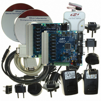
DEV KIT FOR F040/F041/F042/F043
Manufacturer
Silicon Laboratories Inc
Type
MCUr
Specifications of C8051F040DK
Contents
Evaluation Board, Power Supply, USB Cables, Adapter and Documentation
Processor To Be Evaluated
C8051F04x
Interface Type
USB
Silicon Manufacturer
Silicon Labs
Core Architecture
8051
Silicon Core Number
C8051F040
Silicon Family Name
C8051F04x
Lead Free Status / RoHS Status
Contains lead / RoHS non-compliant
For Use With/related Products
Silicon Laboratories C8051 F040, 041, 042, 043 MCUs
Lead Free Status / Rohs Status
Lead free / RoHS Compliant
Other names
336-1205
Available stocks
Company
Part Number
Manufacturer
Quantity
Price
Company:

Part Number:
C8051F040DK
Manufacturer:
SiliconL
Quantity:
9


C8051F040/1/2/3/4/5/6/7
17.2. Ports 4 through 7
On C8051F040/2/4/6 devices, all Port pins on Ports 4 through 7 can be accessed as General-Purpose I/O
(GPIO) pins by reading and writing the associated Port Data registers (See SFR Definition 17.16, SFR
Definition 17.18, SFR Definition 17.20, and SFR Definition 17.22 located on SFR Page F), a set of SFRs
which are both bit and byte-addressable.
A Read of a Port Data register (or Port bit) will always return the logic state present at the pin itself, regard-
less of whether the Crossbar has allocated the pin for peripheral use or not. An exception to this occurs
during the execution of a read-modify-write instruction (ANL, ORL, XRL, CPL, INC, DEC, DJNZ, JBC,
CLR, SET, and the bitwise MOV operation). During the read cycle of the read-modify-write instruction, it is
the contents of the Port Data register, not the state of the Port pins themselves, which is read.
220
Bits7-0:
Bits7-0:
R/W
R/W
Bit7
Bit7
P1MDIN.[7:0]: Port 3 Input Mode Bits.
0: Port Pin is configured in Analog Input mode. The digital input path is disabled (a read from
the Port bit will always return ‘0’). The weak pullup on the pin is disabled.
1: Port Pin is configured in Digital Input mode. A read from the Port bit will return the logic
level at the Pin. The state of the weak pullup is determined by the WEAKPUD bit (XBR2.7,
see SFR Definition 17.3).
P2MDOUT.[7:0]: Port3 Output Mode Bits.
0: Port Pin output mode is configured as Open-Drain.
1: Port Pin output mode is configured as Push-Pull.
R/W
R/W
Bit6
Bit6
SFR Definition 17.15. P3MDOUT: Port3 Output Mode
SFR Definition 17.14. P3MDIN: Port3 Input Mode
R/W
R/W
Bit5
Bit5
R/W
R/W
Bit4
Bit4
Rev. 1.5
R/W
R/W
Bit3
Bit3
R/W
R/W
Bit2
Bit2
R/W
R/W
Bit1
Bit1
SFR Address:
SFR Address:
SFR Page:
SFR Page:
R/W
R/W
Bit0
Bit0
0xA7
F
0xAF
F
00000000
Reset Value
Reset Value
11111111
Related parts for C8051F040DK
Image
Part Number
Description
Manufacturer
Datasheet
Request
R

Part Number:
Description:
SMD/C°/SINGLE-ENDED OUTPUT SILICON OSCILLATOR
Manufacturer:
Silicon Laboratories Inc
Part Number:
Description:
Manufacturer:
Silicon Laboratories Inc
Datasheet:
Part Number:
Description:
N/A N/A/SI4010 AES KEYFOB DEMO WITH LCD RX
Manufacturer:
Silicon Laboratories Inc
Datasheet:
Part Number:
Description:
N/A N/A/SI4010 SIMPLIFIED KEY FOB DEMO WITH LED RX
Manufacturer:
Silicon Laboratories Inc
Datasheet:
Part Number:
Description:
N/A/-40 TO 85 OC/EZLINK MODULE; F930/4432 HIGH BAND (REV E/B1)
Manufacturer:
Silicon Laboratories Inc
Part Number:
Description:
EZLink Module; F930/4432 Low Band (rev e/B1)
Manufacturer:
Silicon Laboratories Inc
Part Number:
Description:
I°/4460 10 DBM RADIO TEST CARD 434 MHZ
Manufacturer:
Silicon Laboratories Inc
Part Number:
Description:
I°/4461 14 DBM RADIO TEST CARD 868 MHZ
Manufacturer:
Silicon Laboratories Inc
Part Number:
Description:
I°/4463 20 DBM RFSWITCH RADIO TEST CARD 460 MHZ
Manufacturer:
Silicon Laboratories Inc
Part Number:
Description:
I°/4463 20 DBM RADIO TEST CARD 868 MHZ
Manufacturer:
Silicon Laboratories Inc
Part Number:
Description:
I°/4463 27 DBM RADIO TEST CARD 868 MHZ
Manufacturer:
Silicon Laboratories Inc
Part Number:
Description:
I°/4463 SKYWORKS 30 DBM RADIO TEST CARD 915 MHZ
Manufacturer:
Silicon Laboratories Inc
Part Number:
Description:
N/A N/A/-40 TO 85 OC/4463 RFMD 30 DBM RADIO TEST CARD 915 MHZ
Manufacturer:
Silicon Laboratories Inc
Part Number:
Description:
I°/4463 20 DBM RADIO TEST CARD 169 MHZ
Manufacturer:
Silicon Laboratories Inc