DO-CPLD-DK-G Xilinx Inc, DO-CPLD-DK-G Datasheet - Page 27
DO-CPLD-DK-G
Manufacturer Part Number
DO-CPLD-DK-G
Description
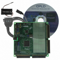
KIT DESIGN CPLD W/BATT HOLDER
Manufacturer
Xilinx Inc
Series
CoolRunner™- IIr
Type
CPLDr
Specifications of DO-CPLD-DK-G
Contents
Proto Board, Download Cable, Samples, Software
For Use With/related Products
CoolRunner-ll, XC9500XL
Lead Free Status / RoHS Status
Lead free / RoHS Compliant
Other names
122-1512
Available stocks
Company
Part Number
Manufacturer
Quantity
Price


Programmable Logic Design
June 12, 2006
I/O Blocks
I/O Banking
DataGATE
R
I/O blocks are primarily transceivers. However, each I/O is either automatically
compliant with standard voltage ranges or can be programmed to become compliant. In
addition to voltage levels, each input can selectively arrive through Schmitt-trigger inputs.
This adds a small time delay, but substantially reduces noise on that input pin. Hysteresis
also allows easy generation of external clock circuits. The Schmitt-trigger path is best
illustrated in
configured. A choice of slow or fast slew rate output signal is also available.
CPLDs are widely used as voltage interface translators; thus, the I/O pins are grouped in
large banks. The four smaller parts have two output banks. With two banks available, the
outputs will switch to one of two selected output voltage levels, unless both banks are set
to the same voltage. The larger parts (384 and 512 macrocell) support four output banks,
split evenly. They can support groupings of one, two, three, or four separate output voltage
levels. This kind of flexibility permits easy interfacing to 3.3V, 2.5V, 1.8V, and 1.5V in a
single part.
Low power is the hallmark of CMOS technology. Other CPLD families use a sense
amplifier approach to create p-terms, which always has a residual current component. This
residual current can be several hundred milliamps, making these CPLDs unusable in
portable systems. CoolRunner-II CPLDs use standard CMOS methods to create the CPLD
architecture and deliver the corresponding low current consumption, without any special
tricks.
However, sometimes you might want to reduce the system current even more by
selectively disabling unused circuitry. The patented DataGATE technology permits a
straightforward approach to additional power reduction. Each I/O pin has a series switch
that can block the arrival of unused free- running signals that may increase power
to Macrocell
to Macrocell
(Fast Input)
(Fast Input)
from Macrocell
from Macrocell
Figure
Control Term
Control Term
Open Drain
Open Drain
Disabled
Disabled
Enabled
Enabled
GTS[0:3]
GTS[0:3]
CGND
CGND
PTB
PTB
to AIM
to AIM
2-8. Outputs can be directly driven, tri-stated, or open-drain
4
4
/
/
Figure 2-8: CoolRunner-II I/O Block
www.xilinx.com
Slewrate
Slewrate
Input Hysteresis
Input Hysteresis
3.3V - 1.5V Input
3.3V - 1.5V Input
V
V
CCIO
CCIO
HSTL & SSTL
HSTL & SSTL
V
V
CCIO
CCIO
V
V
CoolRunner-II Low-Power CPLDs
REF
REF
Weak Pullup/Bus
Weak Pullup/Bus
Weak Pullup/Bus
V
V
128 macrocell
128 macrocell
and larger devices
and larger devices
REF
REF
Hold
Hold
Hold
for Local Bank
for Local Bank
I/O Pin
I/O Pin
I/O Pin
I/O Pin
I/O Pin
I/O Pin
17
Related parts for DO-CPLD-DK-G
Image
Part Number
Description
Manufacturer
Datasheet
Request
R

Part Number:
Description:
STARTER KIT CPLD
Manufacturer:
Xilinx Inc
Datasheet:
Part Number:
Description:
KIT STARTER CPLD JAPANESE
Manufacturer:
Xilinx Inc
Datasheet:
Part Number:
Description:
KIT STARTER CPLD-JAPANESE
Manufacturer:
Xilinx Inc
Datasheet:

Part Number:
Description:
IC CPLD .8K 36MCELL 44-VQFP
Manufacturer:
Xilinx Inc
Datasheet:

Part Number:
Description:
IC CPLD 72MCRCELL 10NS 44VQFP
Manufacturer:
Xilinx Inc
Datasheet:

Part Number:
Description:
IC CPLD 1.6K 72MCELL 64-VQFP
Manufacturer:
Xilinx Inc
Datasheet:

Part Number:
Description:
IC CR-II CPLD 64MCELL 44-VQFP
Manufacturer:
Xilinx Inc
Datasheet:

Part Number:
Description:
IC CPLD 1.6K 72MCELL 100-TQFP
Manufacturer:
Xilinx Inc
Datasheet:

Part Number:
Description:
IC CR-II CPLD 64MCELL 56-BGA
Manufacturer:
Xilinx Inc
Datasheet:

Part Number:
Description:
IC CPLD 72MCRCELL 7.5NS 44VQFP
Manufacturer:
Xilinx Inc
Datasheet:
Part Number:
Description:
IC CR-II CPLD 64MCELL 100-VQFP
Manufacturer:
Xilinx Inc
Datasheet:
Part Number:
Description:
IC CPLD 1.6K 72MCELL 100-TQFP
Manufacturer:
Xilinx Inc
Datasheet:

Part Number:
Description:
IC CPLD 72MCRCELL 7.5NS 64VQFP
Manufacturer:
Xilinx Inc
Datasheet:
Part Number:
Description:
IC CPLD 1.6K 72MCELL 100-TQFP
Manufacturer:
Xilinx Inc
Datasheet:

Part Number:
Description:
IC CPLD 1.5K 64MCELL HP 44-VQFP
Manufacturer:
Xilinx Inc