DSP56309EVM Freescale Semiconductor, DSP56309EVM Datasheet - Page 12
DSP56309EVM
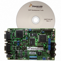
Manufacturer Part Number
DSP56309EVM
Description
KIT EVALUATION FOR XC56309
Manufacturer
Freescale Semiconductor
Type
DSPr
Specifications of DSP56309EVM
Contents
Module Board, Installation Guide, Power Supply, Cable, Software and more
Description/function
Audio DSPs
Product
Audio Modules
For Use With/related Products
DSP56309
Lead Free Status / RoHS Status
Contains lead / RoHS non-compliant


DSP56309 Overview
1.2 Manual Conventions
This manual uses the following conventions:
1-2
Notes: 1.
Chapter 7, Enhanced Synchronous Serial Interface (ESSI). Enhancements, data and
control signals, programming model, operating modes, initialization, exceptions, and
GPIO.
Chapter 8, Serial Communication Interface (SCI). Signals, programming model,
operating modes, reset, initialization, and GPIO.
Chapter 9, Triple Timer Module. Architecture, programming model, and operating modes
of three identical timer devices available for use as internals or event counters.
Appendix A, Bootstrap Code. Bootstrap code and equates for the DSP56309.
Appendix B, Programming Reference. Peripheral addresses, interrupt addresses, and
interrupt priorities for the DSP56309; programming sheets listing the contents of the
major DSP56309 registers for programmer’s reference.
Bits within registers are always listed from most significant bit (MSB) to least significant
bit (LSB).
Bits within a register are indicated AA[n – m], n > m, when more than one bit is involved
in a description. For purposes of description, the bits are presented as if they are
contiguous within a register. However, this is not always the case. Refer to the
programming model diagrams or to the programming sheets to see the exact location of
bits within a register.
When a bit is “set,” its value is 1. When a bit is “cleared,” its value is 0.
The word “assert” means that a high true (active high) signal is pulled high to V
a low true (active low) signal is pulled low to ground. The word “deassert” means that a
high true signal is pulled low to ground or that a low true signal is pulled high to V
Table 1-1.
2.
3.
Signal/Symbol
PIN is a generic term for any pin on the chip.
Ground is an acceptable low voltage level. See the appropriate data sheet for the range of acceptable low
voltage levels (typically a TTL logic low).
V
voltage levels (typically a TTL logic high).
PIN
PIN
PIN
PIN
CC
is an acceptable high voltage level. See the appropriate data sheet for the range of acceptable high
1
Table 1-1. High True/Low True Signal Conventions
DSP56309 User’s Manual, Rev. 1
Logic State
False
False
True
True
Signal State
Deasserted
Deasserted
Asserted
Asserted
Freescale Semiconductor
Ground
Voltage
Ground
V
V
CC
CC
3
CC
2
CC
or that
. See
Related parts for DSP56309EVM
Image
Part Number
Description
Manufacturer
Datasheet
Request
R

Part Number:
Description:
Manufacturer:
Freescale Semiconductor, Inc
Datasheet:
Part Number:
Description:
Manufacturer:
Freescale Semiconductor, Inc
Datasheet:
Part Number:
Description:
Manufacturer:
Freescale Semiconductor, Inc
Datasheet:
Part Number:
Description:
Manufacturer:
Freescale Semiconductor, Inc
Datasheet:
Part Number:
Description:
Manufacturer:
Freescale Semiconductor, Inc
Datasheet:
Part Number:
Description:
Manufacturer:
Freescale Semiconductor, Inc
Datasheet:
Part Number:
Description:
Manufacturer:
Freescale Semiconductor, Inc
Datasheet:
Part Number:
Description:
Manufacturer:
Freescale Semiconductor, Inc
Datasheet:
Part Number:
Description:
Manufacturer:
Freescale Semiconductor, Inc
Datasheet:
Part Number:
Description:
Manufacturer:
Freescale Semiconductor, Inc
Datasheet:
Part Number:
Description:
Manufacturer:
Freescale Semiconductor, Inc
Datasheet:
Part Number:
Description:
Manufacturer:
Freescale Semiconductor, Inc
Datasheet:
Part Number:
Description:
Manufacturer:
Freescale Semiconductor, Inc
Datasheet:
Part Number:
Description:
Manufacturer:
Freescale Semiconductor, Inc
Datasheet:
Part Number:
Description:
Manufacturer:
Freescale Semiconductor, Inc
Datasheet: