DSP56309EVM Freescale Semiconductor, DSP56309EVM Datasheet - Page 235
DSP56309EVM
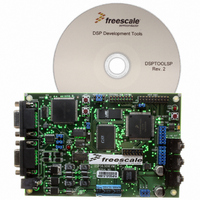
Manufacturer Part Number
DSP56309EVM
Description
KIT EVALUATION FOR XC56309
Manufacturer
Freescale Semiconductor
Type
DSPr
Specifications of DSP56309EVM
Contents
Module Board, Installation Guide, Power Supply, Cable, Software and more
Description/function
Audio DSPs
Product
Audio Modules
For Use With/related Products
DSP56309
Lead Free Status / RoHS Status
Contains lead / RoHS non-compliant


Programming Reference
This reference for programmers includes a table showing the addresses of all DSP
memory-mapped peripherals, an exception priority table, and programming sheets for the major
programmable DSP registers. The programming sheets are grouped in the following order:
central processor, Phase Lock Loop (PLL), Host Interface (HI08), Enhanced Synchronous Serial
Interface (ESSI), Serial Communication Interface (SCI), Timer, and GPIO. Each sheet provides
room to write in the value of each bit and the hexadecimal value for each register. You can
photocopy these sheets and reuse them for each application development project. For details on
the instruction set of the DSP56300 family of DSPs, see the DSP56300 Family Manual.
Freescale Semiconductor
Processor
Module
Central
DMA
PLL
IPR
BIU
addresses of all internal peripherals.
sources.
specific interrupts within interrupt priority levels.
The programming sheets appear in this manual as figures (listed in Table B-1); they show
the major programmable registers on the DSP56309.
Table B-2, Internal I/O Memory Map (X Data Memory), on page B-2 lists the memory
Table B-3, Interrupt Sources, on page B-6 lists the interrupt starting addresses and
Table B-4, Interrupt Source Priorities Within an IPL, on page B-8 lists the priorities of
Figure B-1, Status Register (SR)
Figure B-2, Operating Mode Register (OMR)
Figure B-3, Interrupt Priority Register-Peripherals (IPRP)
Figure B-3, Interrupt Priority Register-Peripherals (IPRP)
Figure B-4, Phase-Locked Loop Control Register (PCTL)
Figure B-5, Bus Control Register (BCR)
Figure B-6, DRAM Control Register (DCR)
Figure B-7, Address Attribute Registers (AAR[3–0])
Figure B-8, DMA Control Registers 5–0 (DCR[5–0])
Table B-1. Guide to Programming Sheets
DSP56309 User’s Manual, Rev. 1
Programming Sheet
page B-10
page B-11
page B-12
page B-12
page B-13
page B-14
page B-15
page B-16
page B-17
Page
B
B-1
Related parts for DSP56309EVM
Image
Part Number
Description
Manufacturer
Datasheet
Request
R

Part Number:
Description:
Manufacturer:
Freescale Semiconductor, Inc
Datasheet:
Part Number:
Description:
Manufacturer:
Freescale Semiconductor, Inc
Datasheet:
Part Number:
Description:
Manufacturer:
Freescale Semiconductor, Inc
Datasheet:
Part Number:
Description:
Manufacturer:
Freescale Semiconductor, Inc
Datasheet:
Part Number:
Description:
Manufacturer:
Freescale Semiconductor, Inc
Datasheet:
Part Number:
Description:
Manufacturer:
Freescale Semiconductor, Inc
Datasheet:
Part Number:
Description:
Manufacturer:
Freescale Semiconductor, Inc
Datasheet:
Part Number:
Description:
Manufacturer:
Freescale Semiconductor, Inc
Datasheet:
Part Number:
Description:
Manufacturer:
Freescale Semiconductor, Inc
Datasheet:
Part Number:
Description:
Manufacturer:
Freescale Semiconductor, Inc
Datasheet:
Part Number:
Description:
Manufacturer:
Freescale Semiconductor, Inc
Datasheet:
Part Number:
Description:
Manufacturer:
Freescale Semiconductor, Inc
Datasheet:
Part Number:
Description:
Manufacturer:
Freescale Semiconductor, Inc
Datasheet:
Part Number:
Description:
Manufacturer:
Freescale Semiconductor, Inc
Datasheet:
Part Number:
Description:
Manufacturer:
Freescale Semiconductor, Inc
Datasheet: