DSP56309EVM Freescale Semiconductor, DSP56309EVM Datasheet - Page 151
DSP56309EVM
Manufacturer Part Number
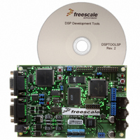
DSP56309EVM
Description
KIT EVALUATION FOR XC56309
Manufacturer
Freescale Semiconductor
Type
DSPr
Specifications of DSP56309EVM
Contents
Module Board, Installation Guide, Power Supply, Cable, Software and more
Description/function
Audio DSPs
Product
Audio Modules
For Use With/related Products
DSP56309
Lead Free Status / RoHS Status
Contains lead / RoHS non-compliant


Freescale Semiconductor
Bit Number
17
16
15
Table 7-4. ESSI Control Register B (CRB) Bit Definitions (Continued)
Bit Name
TE0
TE1
RE
Reset Value
0
0
0
DSP56309 User’s Manual, Rev. 1
Receive Enable
Enables/disables the receive portion of the ESSI. When RE is cleared, the
receiver is disabled: data transfer into RX is inhibited. If data is being
received while this bit is cleared, the remainder of the word is shifted in and
transferred to the ESSI receive data register. RE must be set in both
Normal and On-Demand modes for the ESSI to receive data. In Network
mode, clearing RE and setting it again disables the receiver after reception
of the current data word. The receiver remains disabled until the beginning
of the next data frame.
Note:
Transmit 0 Enable
Enables the transfer of data from TX0 to Transmit Shift Register 0. TE0 is
functional when the ESSI is in either synchronous or Asynchronous mode.
When TE0 is set and a frame sync is detected, the transmitter 0 is enabled
for that frame.
When TE0 is cleared, transmitter 0 is disabled after the transmission of data
currently in the ESSI transmit shift register. The STD output is tri-stated,
and any data present in TX0 is not transmitted. In other words, data can be
written to TX0 with TE0 cleared; the TDE bit is cleared, but data is not
transferred to the transmit shift register 0. The transmit enable sequence in
On-Demand mode can be the same as in Normal mode, or TE0 can be left
enabled.
Note:
Transmit 1 Enable
Enables the transfer of data from TX1 to Transmit Shift Register 1. TE1 is
functional only when the ESSI is in Synchronous mode and is ignored when
the ESSI is in Asynchronous mode. When TE1 is set and a frame sync is
detected, transmitter 1 is enabled for that frame.
When TE1 is cleared, transmitter 1 is disabled after completing
transmission of data currently in the ESSI transmit shift register. Any data
present in TX1 is not transmitted. If TE1 is cleared, data can be written to
TX1; the TDE bit is cleared, but data is not transferred to transmit shift
register 1. If the TE1 bit is kept cleared until the start of the next frame, it
causes the SC0 signal to act as serial I/O flag from the start of the frame in
both Normal and Network mode. The transmit enable sequence in
On-Demand mode can be the same as in Normal mode, or the TE1 bit can
be left enabled.
Note:
The setting of the RE bit does not affect the generation of a frame
sync.
Transmitter 0 is the only transmitter that can operate in
Asynchronous mode (SYN = 0). The setting of the TE0 bit does
not affect the generation of frame sync or output flags.
The setting of the TE1 bit does not affect the generation of frame
sync or output flags.
Description
ESSI Programming Model
7-19
Related parts for DSP56309EVM
Image
Part Number
Description
Manufacturer
Datasheet
Request
R

Part Number:
Description:
Manufacturer:
Freescale Semiconductor, Inc
Datasheet:
Part Number:
Description:
Manufacturer:
Freescale Semiconductor, Inc
Datasheet:
Part Number:
Description:
Manufacturer:
Freescale Semiconductor, Inc
Datasheet:
Part Number:
Description:
Manufacturer:
Freescale Semiconductor, Inc
Datasheet:
Part Number:
Description:
Manufacturer:
Freescale Semiconductor, Inc
Datasheet:
Part Number:
Description:
Manufacturer:
Freescale Semiconductor, Inc
Datasheet:
Part Number:
Description:
Manufacturer:
Freescale Semiconductor, Inc
Datasheet:
Part Number:
Description:
Manufacturer:
Freescale Semiconductor, Inc
Datasheet:
Part Number:
Description:
Manufacturer:
Freescale Semiconductor, Inc
Datasheet:
Part Number:
Description:
Manufacturer:
Freescale Semiconductor, Inc
Datasheet:
Part Number:
Description:
Manufacturer:
Freescale Semiconductor, Inc
Datasheet:
Part Number:
Description:
Manufacturer:
Freescale Semiconductor, Inc
Datasheet:
Part Number:
Description:
Manufacturer:
Freescale Semiconductor, Inc
Datasheet:
Part Number:
Description:
Manufacturer:
Freescale Semiconductor, Inc
Datasheet:
Part Number:
Description:
Manufacturer:
Freescale Semiconductor, Inc
Datasheet: