DSP56309EVM Freescale Semiconductor, DSP56309EVM Datasheet - Page 46
DSP56309EVM
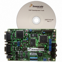
Manufacturer Part Number
DSP56309EVM
Description
KIT EVALUATION FOR XC56309
Manufacturer
Freescale Semiconductor
Type
DSPr
Specifications of DSP56309EVM
Contents
Module Board, Installation Guide, Power Supply, Cable, Software and more
Description/function
Audio DSPs
Product
Audio Modules
For Use With/related Products
DSP56309
Lead Free Status / RoHS Status
Contains lead / RoHS non-compliant


Memory Configuration
3.1.1 Internal Program Memory
The default internal program memory consists of a 24-bit-wide, high-speed, SRAM occupying
the lowest 20 K (default), 19 K, 24 K, or 24 K locations in program memory space, depending on
the settings of the OMR[MS] and (SR[CE]) bits. Section 4.3.2, Operating Mode Register (OMR),
on page 4-12 provides details on the MS bit. Section 4.3.1, Status Register (SR), on page 4-7
provides details on the CE bit. The default internal program RAM is organized in 80 banks with
256 locations each (20 K). Setting the MS bit switches eight banks of the X data memory and an
additional eight banks of the Y data memory to program memory. Setting the CE bit switches
four banks of internal program memory to the Instruction Cache and reassigns its address to
external program memory. The memory addresses for the Instruction Cache vary depending on
the setting of the MS and CE bits. Section 3.6 provides a summary of the internal RAM
configurations. Refer to the memory maps for detailed information.
3.1.2 Memory Switch Modes—Program Memory
Memory switch mode allows reallocation of portions of program RAM to X and Y data RAM.
OMR[7] is the memory switch (MS) bit that controls this function, as follows:
3.1.3 Instruction Cache
In program memory space, the location of the internal Instruction Cache (when enabled by the
CE bit) varies depending on the setting of the MS bit, as noted above. Refer to the memory maps
for detailed address information. When the instruction cache is enabled (that is, the SR[CE] bit is
set), 1 K program words switch to instruction cache and are not accessible via addressing; the
address range switches to external program memory.
3.1.4 Program Bootstrap ROM
The program memory space occupying locations $FF0000–$FF00BF includes the internal
bootstrap ROM. This ROM contains the 192-word DSP56309 bootstrap program.
3-2
When the MS bit is cleared, program memory consists of the default 20 K × 24-bit
memory space described in the previous section. In this default mode, the lowest external
program memory location is $5000. If the CE bit is set, the program memory consists of
the lowest 19 K × 24-bits of memory space.
When the MS bit is set, the highest 2 K × 24-bit portion of both the X data memory and
the Y data memory is switched to internal program memory, yielding a total of 24 K ×
24-bit program memory space. In this mode, the lowest external program memory location
is $6000. If the CE bit is set and the MS bit is set, the program memory is 23 K × 24-bits.
DSP56309 User’s Manual, Rev. 1
Freescale Semiconductor
Related parts for DSP56309EVM
Image
Part Number
Description
Manufacturer
Datasheet
Request
R

Part Number:
Description:
Manufacturer:
Freescale Semiconductor, Inc
Datasheet:
Part Number:
Description:
Manufacturer:
Freescale Semiconductor, Inc
Datasheet:
Part Number:
Description:
Manufacturer:
Freescale Semiconductor, Inc
Datasheet:
Part Number:
Description:
Manufacturer:
Freescale Semiconductor, Inc
Datasheet:
Part Number:
Description:
Manufacturer:
Freescale Semiconductor, Inc
Datasheet:
Part Number:
Description:
Manufacturer:
Freescale Semiconductor, Inc
Datasheet:
Part Number:
Description:
Manufacturer:
Freescale Semiconductor, Inc
Datasheet:
Part Number:
Description:
Manufacturer:
Freescale Semiconductor, Inc
Datasheet:
Part Number:
Description:
Manufacturer:
Freescale Semiconductor, Inc
Datasheet:
Part Number:
Description:
Manufacturer:
Freescale Semiconductor, Inc
Datasheet:
Part Number:
Description:
Manufacturer:
Freescale Semiconductor, Inc
Datasheet:
Part Number:
Description:
Manufacturer:
Freescale Semiconductor, Inc
Datasheet:
Part Number:
Description:
Manufacturer:
Freescale Semiconductor, Inc
Datasheet:
Part Number:
Description:
Manufacturer:
Freescale Semiconductor, Inc
Datasheet:
Part Number:
Description:
Manufacturer:
Freescale Semiconductor, Inc
Datasheet: