DSP56309EVM Freescale Semiconductor, DSP56309EVM Datasheet - Page 171
DSP56309EVM
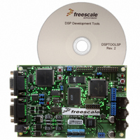
Manufacturer Part Number
DSP56309EVM
Description
KIT EVALUATION FOR XC56309
Manufacturer
Freescale Semiconductor
Type
DSPr
Specifications of DSP56309EVM
Contents
Module Board, Installation Guide, Power Supply, Cable, Software and more
Description/function
Audio DSPs
Product
Audio Modules
For Use With/related Products
DSP56309
Lead Free Status / RoHS Status
Contains lead / RoHS non-compliant


I/O Signals
8.1.3.1 Transmitting Data and Address Characters
To send data, the 8-bit data character must be written to the STX register. Writing the data
character to the STX register sets the ninth bit in the frame to zero, which indicates that this frame
contains data. To send an 8-bit address, the address data is written to the STXA register, and the
ninth bit in the frame is set to one, indicating that this frame contains an address.
8.1.3.2 Wired-OR Mode
Building a multidrop bus network requires connecting multiple transmitters to a common wire.
The Wired-OR mode allows this to be done without damaging the transmitters when the
transmitters are not in use. A protocol is still needed to prevent two transmitters from
simultaneously driving the bus. The SCI multidrop word format provides an address field to
support this protocol.
8.1.3.3 Idle Line Wakeup
A wakeup mode frees a DSP from reading messages intended for other processors. The usual
operational procedure is for each DSP to suspend SCI reception (the DSP can continue
processing) until the beginning of a message. Each DSP compares the address in the message
header with the DSP’s address. If the addresses do not match, the SCI again suspends reception
until the next address. If the address matches, the DSP reads and processes the message and then
suspends reception until the next address. The Idle Line Wakeup mode wakes up the SCI to read
a message before the first character arrives.
8.1.3.4 Address Mode Wakeup
The purpose and basic operational procedure for Address Mode Wakeup is the same as for Idle
Line Wakeup. The difference is that Address Mode Wakeup re-enables the SCI when the ninth
bit in a character is set to one (if cleared, this bit marks a character as data; if set, an address). As
a result, an idle line is not needed, which eliminates the dead time between messages.
8.2 I/O Signals
Each of the three SCI signals (
,
, and
) can be configured as either a GPIO signal or
RXD
TXD
SCLK
as a specific SCI signal. Each signal is independent of the others. For example, if only the
TXD
signal is needed, the
and
signals can be programmed for GPIO. However, at least one
RXD
SCLK
of the three signals must be selected as an SCI signal to release the SCI from reset.
To enable SCI interrupts, program the SCI control registers before any of the SCI signals are
programmed as SCI functions. In this case, only one transmit interrupt can be generated because
the Transmit Data Register is empty. The timer and timer interrupt operate regardless of how the
SCI pins are configured, either as SCI or GPIO.
DSP56309 User’s Manual, Rev. 1
Freescale Semiconductor
8-3
Related parts for DSP56309EVM
Image
Part Number
Description
Manufacturer
Datasheet
Request
R

Part Number:
Description:
Manufacturer:
Freescale Semiconductor, Inc
Datasheet:
Part Number:
Description:
Manufacturer:
Freescale Semiconductor, Inc
Datasheet:
Part Number:
Description:
Manufacturer:
Freescale Semiconductor, Inc
Datasheet:
Part Number:
Description:
Manufacturer:
Freescale Semiconductor, Inc
Datasheet:
Part Number:
Description:
Manufacturer:
Freescale Semiconductor, Inc
Datasheet:
Part Number:
Description:
Manufacturer:
Freescale Semiconductor, Inc
Datasheet:
Part Number:
Description:
Manufacturer:
Freescale Semiconductor, Inc
Datasheet:
Part Number:
Description:
Manufacturer:
Freescale Semiconductor, Inc
Datasheet:
Part Number:
Description:
Manufacturer:
Freescale Semiconductor, Inc
Datasheet:
Part Number:
Description:
Manufacturer:
Freescale Semiconductor, Inc
Datasheet:
Part Number:
Description:
Manufacturer:
Freescale Semiconductor, Inc
Datasheet:
Part Number:
Description:
Manufacturer:
Freescale Semiconductor, Inc
Datasheet:
Part Number:
Description:
Manufacturer:
Freescale Semiconductor, Inc
Datasheet:
Part Number:
Description:
Manufacturer:
Freescale Semiconductor, Inc
Datasheet:
Part Number:
Description:
Manufacturer:
Freescale Semiconductor, Inc
Datasheet: