DSP56309EVM Freescale Semiconductor, DSP56309EVM Datasheet - Page 249
DSP56309EVM
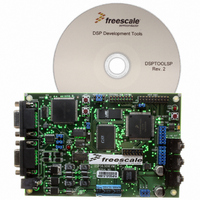
Manufacturer Part Number
DSP56309EVM
Description
KIT EVALUATION FOR XC56309
Manufacturer
Freescale Semiconductor
Type
DSPr
Specifications of DSP56309EVM
Contents
Module Board, Installation Guide, Power Supply, Cable, Software and more
Description/function
Audio DSPs
Product
Audio Modules
For Use With/related Products
DSP56309
Lead Free Status / RoHS Status
Contains lead / RoHS non-compliant


Freescale Semiconductor
Application:
DRAM Control Register (DCR)
Reset = $000000
BRP
NOTE: All DCR bits are read/write control bits.
23 22 21 20
Refresh Prescaler, Bit 23
0 = Prescaler bypassed
1 = Divide-by-64 prescaler used
Bus Interface Unit
Refresh Request Rate, Bits 22–15
These read/write control bits define
the refresh request rate. The bits
specify a divide from 1–256
(BRF[7–0] = $00–$FF). A refresh
request is generated every time
the refresh counter reaches zero,
if the refresh counter is enabled
(i.e., BREN = 1).
19 18 17 16
BRF[7–0]
Figure B-6. DRAM Control Register (DCR)
Bus Software Triggered
Refresh, Bit 14
0 = Refresh complete/reset
1 = Software triggered refresh request
15 14 13 12 11 10 9
DSP56309 User’s Manual, Rev. 1
BSTR BREN BME BPLE
X:$FFFFFA Read/Write
Bus Refresh
Enable, Bit 13
0 = Disable
1 = Enable
Bus Mastership
Enable, Bit 12
0 = Disable
1 = Enable
Bus Page Logic
Enable, Bit 11
0 = Disable
1 = Enable
*
Bus DRAM Page Size, Bits 9–8
0
00 = 9-bit column width, 512
01 = 10-bit column width, 1 K
10 = 11-bit column width, 2 K
11 = 12-bit column width, 4 K
BPS[1–0]
8
*
0
7
*
Bus Row Out-of-Page
Wait States, Bits 3–2
*
00 = 4 wait states
01 = 8 wait states
10 = 11 wait states
11 = 15 wait states
0
Date:
Programmer:
6
= Reserved, Program as 0
*
0
5
*
0
4
Bus In-Page
Wait States, Bits 1–0
00 = 1 wait state
01 = 2 wait states
10 = 3 wait states
11 = 4 wait states
3
BRW[1–0]
Programming Sheets
Sheet 2 of 3
2
BCW[1–0]
1
0
B-15
Related parts for DSP56309EVM
Image
Part Number
Description
Manufacturer
Datasheet
Request
R

Part Number:
Description:
Manufacturer:
Freescale Semiconductor, Inc
Datasheet:
Part Number:
Description:
Manufacturer:
Freescale Semiconductor, Inc
Datasheet:
Part Number:
Description:
Manufacturer:
Freescale Semiconductor, Inc
Datasheet:
Part Number:
Description:
Manufacturer:
Freescale Semiconductor, Inc
Datasheet:
Part Number:
Description:
Manufacturer:
Freescale Semiconductor, Inc
Datasheet:
Part Number:
Description:
Manufacturer:
Freescale Semiconductor, Inc
Datasheet:
Part Number:
Description:
Manufacturer:
Freescale Semiconductor, Inc
Datasheet:
Part Number:
Description:
Manufacturer:
Freescale Semiconductor, Inc
Datasheet:
Part Number:
Description:
Manufacturer:
Freescale Semiconductor, Inc
Datasheet:
Part Number:
Description:
Manufacturer:
Freescale Semiconductor, Inc
Datasheet:
Part Number:
Description:
Manufacturer:
Freescale Semiconductor, Inc
Datasheet:
Part Number:
Description:
Manufacturer:
Freescale Semiconductor, Inc
Datasheet:
Part Number:
Description:
Manufacturer:
Freescale Semiconductor, Inc
Datasheet:
Part Number:
Description:
Manufacturer:
Freescale Semiconductor, Inc
Datasheet:
Part Number:
Description:
Manufacturer:
Freescale Semiconductor, Inc
Datasheet: