DSP56309EVM Freescale Semiconductor, DSP56309EVM Datasheet - Page 30
DSP56309EVM
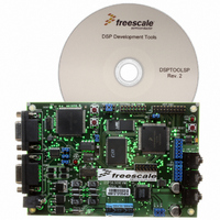
Manufacturer Part Number
DSP56309EVM
Description
KIT EVALUATION FOR XC56309
Manufacturer
Freescale Semiconductor
Type
DSPr
Specifications of DSP56309EVM
Contents
Module Board, Installation Guide, Power Supply, Cable, Software and more
Description/function
Audio DSPs
Product
Audio Modules
For Use With/related Products
DSP56309
Lead Free Status / RoHS Status
Contains lead / RoHS non-compliant


Signals/Connections
2.5.2 External Data Bus
2.5.3 External Bus Control
2-6
AA0/RAS0–
AA3/RAS3
RD
WR
TA
D[0–23]
Signal
Name
Signal
Name
Input/Output
Output
Output
Output
Input
Type
Type
Tri-stated
Tri-stated
Tri-stated
Ignored Input
State During Reset,
Tri-stated
State During Reset,
Stop, or Wait
Stop, or Wait
Table 2-8. External Bus Control Signals
Table 2-7. External Data Bus Signals
DSP56309 User’s Manual, Rev. 1
Address Attribute or Row Address Strobe
As AA, these signals function as chip selects or additional address lines.
Unlike address lines, however, the AA lines do not hold their state after a
read or write operation. As RAS, these signals can be used for Dynamic
Random Access Memory (DRAM) interface. These signals have
programmable polarity.
Read Enable
When the DSP is the bus master, RD is asserted to read external memory
on the data bus (D[0–23]). Otherwise, RD is tri-stated.
Write Enable
When the DSP is the bus master, WR is asserted to write external
memory on the data bus (D[0–23]). Otherwise, WR is tri-stated.
Transfer Acknowledge
If the DSP56309 is the bus master and there is no external bus activity, or
the DSP56309 is not the bus master, the
is a Data Transfer Acknowledge (DTACK) function that can extend an
external bus cycle indefinitely. Any number of wait states (1, 2,..., infinity)
can be added to the wait states inserted by the BCR by keeping TA
deasserted. In typical operation,
cycle, asserted to enable completion of the bus cycle, and deasserted
before the next bus cycle. The current bus cycle completes one clock
period after TA is asserted synchronous to CLKOUT. The number of wait
states is determined by the TA input or by the Bus Control Register (BCR),
whichever is longer. The BCR can set the minimum number of wait states
in external bus cycles.
To use the TA functionality, the BCR must be programmed to at least one
wait state. A zero wait state access cannot be extended by TA
deassertion; otherwise improper operation may result.
synchronously or asynchronously, depending on the setting of the TAS bit
in the Operating Mode Register (OMR).
TA functionality cannot be used during DRAM-type accesses; otherwise
improper operation may result.
Data Bus
When the DSP is the bus master, D[0–23] provide the bidirectional
data bus for external program and data memory accesses. Otherwise,
D[0–23] are tri-stated.
Signal Description
Signal Description
TA
is deasserted at the start of a bus
TA
input is ignored. The TA input
Freescale Semiconductor
TA
can operate
Related parts for DSP56309EVM
Image
Part Number
Description
Manufacturer
Datasheet
Request
R

Part Number:
Description:
Manufacturer:
Freescale Semiconductor, Inc
Datasheet:
Part Number:
Description:
Manufacturer:
Freescale Semiconductor, Inc
Datasheet:
Part Number:
Description:
Manufacturer:
Freescale Semiconductor, Inc
Datasheet:
Part Number:
Description:
Manufacturer:
Freescale Semiconductor, Inc
Datasheet:
Part Number:
Description:
Manufacturer:
Freescale Semiconductor, Inc
Datasheet:
Part Number:
Description:
Manufacturer:
Freescale Semiconductor, Inc
Datasheet:
Part Number:
Description:
Manufacturer:
Freescale Semiconductor, Inc
Datasheet:
Part Number:
Description:
Manufacturer:
Freescale Semiconductor, Inc
Datasheet:
Part Number:
Description:
Manufacturer:
Freescale Semiconductor, Inc
Datasheet:
Part Number:
Description:
Manufacturer:
Freescale Semiconductor, Inc
Datasheet:
Part Number:
Description:
Manufacturer:
Freescale Semiconductor, Inc
Datasheet:
Part Number:
Description:
Manufacturer:
Freescale Semiconductor, Inc
Datasheet:
Part Number:
Description:
Manufacturer:
Freescale Semiconductor, Inc
Datasheet:
Part Number:
Description:
Manufacturer:
Freescale Semiconductor, Inc
Datasheet:
Part Number:
Description:
Manufacturer:
Freescale Semiconductor, Inc
Datasheet: