DSP56309EVM Freescale Semiconductor, DSP56309EVM Datasheet - Page 17
DSP56309EVM
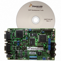
Manufacturer Part Number
DSP56309EVM
Description
KIT EVALUATION FOR XC56309
Manufacturer
Freescale Semiconductor
Type
DSPr
Specifications of DSP56309EVM
Contents
Module Board, Installation Guide, Power Supply, Cable, Software and more
Description/function
Audio DSPs
Product
Audio Modules
For Use With/related Products
DSP56309
Lead Free Status / RoHS Status
Contains lead / RoHS non-compliant


contents of either the A or B accumulator. A 56-bit result can be stored as a 24-bit operand. The
LSP is either truncated or rounded into the MSP. Rounding is performed if specified.
1.6.2 Address Generation Unit (AGU)
The AGU performs the effective address calculations using integer arithmetic necessary to
address data operands in memory and contains the registers that generate the addresses. It
implements four types of arithmetic: linear, modulo, multiple wrap-around modulo, and
reverse-carry. The AGU operates in parallel with other chip resources to minimize
address-generation overhead.
The AGU is divided into halves, each with its own identical address ALU. Each address ALU has
four sets of register triplets, and each register triplet includes an address register, offset register,
and modifier register. Each contains a 24-bit full adder (called an offset adder). A second full
adder (called a modulo adder) adds the summed result of the first full adder to a modulo value
that is stored in its respective modifier register. A third full adder (called a reverse-carry adder) is
also provided. The offset adder and the reverse-carry adder work in parallel and share common
inputs. The only difference between them is that the carry propagates in opposite directions. Test
logic determines which of the three summed results of the full adders is output.
Each address ALU can update one address register from its own address register file during one
instruction cycle. The contents of the associated modifier register specify the type of arithmetic
used in the address register update calculation. The modifier value is decoded in the address
ALU.
1.6.3 Program Control Unit (PCU)
The PCU fetches and decodes instructions, controls hardware DO loops, and processes
exceptions. Its seven-stage pipeline controls the different processing states of the DSP56300
core. The PCU consists of three hardware blocks:
PCU features include the following:
Freescale Semiconductor
Program decode controller. Decodes the 24-bit instruction loaded into the instruction
latch and generates all signals for pipeline control.
Program address generator. Contains all the hardware needed for program address
generation, system stack, and loop control.
Program interrupt controller. Arbitrates among all interrupt requests (internal interrupts,
as well as the five external requests
appropriate interrupt vector address.
Position-independent code support
Addressing modes optimized for DSP applications (including immediate offsets)
Instruction cache controller
DSP56309 User’s Manual, Rev. 1
IRQA
,
IRQB
,
IRQC
,
IRQD
, and
DSP56300 Core Functional Blocks
NMI
), and generates the
1-7
Related parts for DSP56309EVM
Image
Part Number
Description
Manufacturer
Datasheet
Request
R

Part Number:
Description:
Manufacturer:
Freescale Semiconductor, Inc
Datasheet:
Part Number:
Description:
Manufacturer:
Freescale Semiconductor, Inc
Datasheet:
Part Number:
Description:
Manufacturer:
Freescale Semiconductor, Inc
Datasheet:
Part Number:
Description:
Manufacturer:
Freescale Semiconductor, Inc
Datasheet:
Part Number:
Description:
Manufacturer:
Freescale Semiconductor, Inc
Datasheet:
Part Number:
Description:
Manufacturer:
Freescale Semiconductor, Inc
Datasheet:
Part Number:
Description:
Manufacturer:
Freescale Semiconductor, Inc
Datasheet:
Part Number:
Description:
Manufacturer:
Freescale Semiconductor, Inc
Datasheet:
Part Number:
Description:
Manufacturer:
Freescale Semiconductor, Inc
Datasheet:
Part Number:
Description:
Manufacturer:
Freescale Semiconductor, Inc
Datasheet:
Part Number:
Description:
Manufacturer:
Freescale Semiconductor, Inc
Datasheet:
Part Number:
Description:
Manufacturer:
Freescale Semiconductor, Inc
Datasheet:
Part Number:
Description:
Manufacturer:
Freescale Semiconductor, Inc
Datasheet:
Part Number:
Description:
Manufacturer:
Freescale Semiconductor, Inc
Datasheet:
Part Number:
Description:
Manufacturer:
Freescale Semiconductor, Inc
Datasheet: