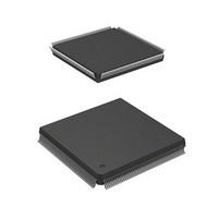
HD6417750RF200DV Renesas Electronics America, HD6417750RF200DV Datasheet - Page 282

HD6417750RF200DV
Manufacturer Part Number
HD6417750RF200DV
Description
MPU 1.5/3.3V 0K I-TEMP PB-FREE 2
Manufacturer
Renesas Electronics America
Series
SuperH® SH7750r
Datasheet
1.D6417750RBP240DV.pdf
(1164 pages)
Specifications of HD6417750RF200DV
Core Processor
SH-4
Core Size
32-Bit
Speed
200MHz
Connectivity
EBI/EMI, FIFO, SCI, SmartCard
Peripherals
DMA, POR, WDT
Number Of I /o
28
Program Memory Type
ROMless
Ram Size
48K x 8
Voltage - Supply (vcc/vdd)
1.35 V ~ 1.6 V
Oscillator Type
External
Operating Temperature
-40°C ~ 85°C
Package / Case
208-QFP Exposed Pad, 208-eQFP, 208-HQFP
Lead Free Status / RoHS Status
Lead free / RoHS Compliant
Eeprom Size
-
Program Memory Size
-
Data Converters
-
Available stocks
Company
Part Number
Manufacturer
Quantity
Price
Company:
Part Number:
HD6417750RF200DV
Manufacturer:
FREESCALE
Quantity:
450
- Current page: 282 of 1164
- Download datasheet (7Mb)
Section 6 Floating-Point Unit (FPU)
Since approximate-value computations are performed to enable high-speed computation, the
inexact exception (I) bit in the cause field and flag field is always set to 1 when an FIPR
instruction is executed. Therefore, if the corresponding bit is set in the enable field, enable
exception handling will be executed.
FTRV XMTRX, FVn (n: 0, 4, 8, 12): This instruction is basically used for the following
purposes:
• Matrix (4 × 4) ⋅ vector (4):
• Matrix (4 × 4) × matrix (4 × 4):
Since approximate-value computations are performed to enable high-speed computation, the
inexact exception (I) bit in the cause field and flag field is always set to 1 when an FTRV
instruction is executed. Therefore, if the corresponding bit is set in the enable field, enable
exception handling will be executed. For the same reason, it is not possible to check all data types
in the registers beforehand when executing an FTRV instruction. If the V bit is set in the enable
field, enable exception handling will be executed.
FRCHG: This instruction modifies banked registers. For example, when the FTRV instruction is
executed, matrix elements must be set in an array in the background bank. However, to create the
actual elements of a translation matrix, it is easier to use registers in the foreground bank. When
the LDC instruction is used on FPSCR, this instruction expends 4 to 5 cycles in order to maintain
the FPU state. With the FRCHG instruction, an FPSCR.FR bit modification can be performed in
one cycle.
6.6.2
In addition to the geometric operation instructions, the FPU also supports high-speed data transfer
instructions.
When FPSCR.SZ = 1, the FPU can perform data transfer by means of pair single-precision data
transfer instructions.
• FMOV DRm/XDm, DRn/XDRn (m, n: 0, 2, 4, 6, 8, 10, 12, 14)
• FMOV DRm/XDm, @Rn (m: 0, 2, 4, 6, 8, 10, 12, 14; n: 0 to 15)
Rev.7.00 Oct. 10, 2008 Page 196 of 1074
REJ09B0366-0700
This operation is generally used for viewpoint changes, angle changes, or movements called
vector transformations (4-dimensional). Since affine transformation processing for angle +
parallel movement basically requires a 4 × 4 matrix, the FPU supports 4-dimensional
operations.
This operation requires the execution of four FTRV instructions.
Pair Single-Precision Data Transfer
Related parts for HD6417750RF200DV
Image
Part Number
Description
Manufacturer
Datasheet
Request
R

Part Number:
Description:
KIT STARTER FOR M16C/29
Manufacturer:
Renesas Electronics America
Datasheet:

Part Number:
Description:
KIT STARTER FOR R8C/2D
Manufacturer:
Renesas Electronics America
Datasheet:

Part Number:
Description:
R0K33062P STARTER KIT
Manufacturer:
Renesas Electronics America
Datasheet:

Part Number:
Description:
KIT STARTER FOR R8C/23 E8A
Manufacturer:
Renesas Electronics America
Datasheet:

Part Number:
Description:
KIT STARTER FOR R8C/25
Manufacturer:
Renesas Electronics America
Datasheet:

Part Number:
Description:
KIT STARTER H8S2456 SHARPE DSPLY
Manufacturer:
Renesas Electronics America
Datasheet:

Part Number:
Description:
KIT STARTER FOR R8C38C
Manufacturer:
Renesas Electronics America
Datasheet:

Part Number:
Description:
KIT STARTER FOR R8C35C
Manufacturer:
Renesas Electronics America
Datasheet:

Part Number:
Description:
KIT STARTER FOR R8CL3AC+LCD APPS
Manufacturer:
Renesas Electronics America
Datasheet:

Part Number:
Description:
KIT STARTER FOR RX610
Manufacturer:
Renesas Electronics America
Datasheet:

Part Number:
Description:
KIT STARTER FOR R32C/118
Manufacturer:
Renesas Electronics America
Datasheet:

Part Number:
Description:
KIT DEV RSK-R8C/26-29
Manufacturer:
Renesas Electronics America
Datasheet:

Part Number:
Description:
KIT STARTER FOR SH7124
Manufacturer:
Renesas Electronics America
Datasheet:

Part Number:
Description:
KIT STARTER FOR H8SX/1622
Manufacturer:
Renesas Electronics America
Datasheet:

Part Number:
Description:
KIT DEV FOR SH7203
Manufacturer:
Renesas Electronics America
Datasheet:


