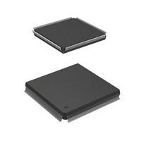
HD6417750RF200DV Renesas Electronics America, HD6417750RF200DV Datasheet - Page 626

HD6417750RF200DV
Manufacturer Part Number
HD6417750RF200DV
Description
MPU 1.5/3.3V 0K I-TEMP PB-FREE 2
Manufacturer
Renesas Electronics America
Series
SuperH® SH7750r
Datasheet
1.D6417750RBP240DV.pdf
(1164 pages)
Specifications of HD6417750RF200DV
Core Processor
SH-4
Core Size
32-Bit
Speed
200MHz
Connectivity
EBI/EMI, FIFO, SCI, SmartCard
Peripherals
DMA, POR, WDT
Number Of I /o
28
Program Memory Type
ROMless
Ram Size
48K x 8
Voltage - Supply (vcc/vdd)
1.35 V ~ 1.6 V
Oscillator Type
External
Operating Temperature
-40°C ~ 85°C
Package / Case
208-QFP Exposed Pad, 208-eQFP, 208-HQFP
Lead Free Status / RoHS Status
Lead free / RoHS Compliant
Eeprom Size
-
Program Memory Size
-
Data Converters
-
Available stocks
Company
Part Number
Manufacturer
Quantity
Price
Company:
Part Number:
HD6417750RF200DV
Manufacturer:
FREESCALE
Quantity:
450
- Current page: 626 of 1164
- Download datasheet (7Mb)
Section 13 Bus State Controller (BSC)
If a refresh request is generated when BACK has been asserted and the bus has been released, the
BACK signal is negated even while the BREQ signal is asserted to request the slave to relinquish
the bus. When this LSI is used in master mode, consecutive bus accesses may be attempted to
reduce the overhead due to arbitration in the case of a slave designed independently by the user.
When connecting a slave for which the total duration of consecutive accesses exceeds the refresh
cycle, the design should provide for the bus to be released as soon as possible after negation of the
BACK signal is detected.
13.3.13 Slave Mode
In slave mode, the bus is normally in the released state, and an external device cannot be accessed
unless the bus is acquired through execution of the bus arbitration sequence. In a reset, also, the
bus-released state is established and the bus arbitration sequence is started from the reset vector
fetch.
To acquire the bus, the slave device asserts (drives low) the BSREQ signal in synchronization
with the rising edge of the clock. The bus use permission BSACK signal is sampled for assertion
(low level) in synchronization with the rising edge of the clock. When BSACK assertion is
detected, the bus control signals and address bus are immediately driven at the negated level. The
bus cycle is started at the next rising edge of the clock. The last signal negated at the end of the
access cycle is synchronized with the rising edge of the clock. When the bus cycle ends, the
BSREQ signal is negated and the release of the bus is reported to the master. On the next rising
edge of the clock, the control signals are set to high-impedance.
In order for the slave mode processor to begin access, the BSACK signal must be asserted for at
least two cycles.
For a slave access cycle in DRAM or synchronous DRAM, the bus is released on completion of
precharging, as in the case of the master.
Refresh control is left to the master mode device, and any refresh control settings made in slave
mode are ignored.
Do not use DRAM/synchronous DRAM RAS down mode in slave mode.
Synchronous DRAM mode register settings should be made by the master mode device. Do not
use the DMAC's DDT mode in slave mode.
Rev.7.00 Oct. 10, 2008 Page 540 of 1074
REJ09B0366-0700
Related parts for HD6417750RF200DV
Image
Part Number
Description
Manufacturer
Datasheet
Request
R

Part Number:
Description:
KIT STARTER FOR M16C/29
Manufacturer:
Renesas Electronics America
Datasheet:

Part Number:
Description:
KIT STARTER FOR R8C/2D
Manufacturer:
Renesas Electronics America
Datasheet:

Part Number:
Description:
R0K33062P STARTER KIT
Manufacturer:
Renesas Electronics America
Datasheet:

Part Number:
Description:
KIT STARTER FOR R8C/23 E8A
Manufacturer:
Renesas Electronics America
Datasheet:

Part Number:
Description:
KIT STARTER FOR R8C/25
Manufacturer:
Renesas Electronics America
Datasheet:

Part Number:
Description:
KIT STARTER H8S2456 SHARPE DSPLY
Manufacturer:
Renesas Electronics America
Datasheet:

Part Number:
Description:
KIT STARTER FOR R8C38C
Manufacturer:
Renesas Electronics America
Datasheet:

Part Number:
Description:
KIT STARTER FOR R8C35C
Manufacturer:
Renesas Electronics America
Datasheet:

Part Number:
Description:
KIT STARTER FOR R8CL3AC+LCD APPS
Manufacturer:
Renesas Electronics America
Datasheet:

Part Number:
Description:
KIT STARTER FOR RX610
Manufacturer:
Renesas Electronics America
Datasheet:

Part Number:
Description:
KIT STARTER FOR R32C/118
Manufacturer:
Renesas Electronics America
Datasheet:

Part Number:
Description:
KIT DEV RSK-R8C/26-29
Manufacturer:
Renesas Electronics America
Datasheet:

Part Number:
Description:
KIT STARTER FOR SH7124
Manufacturer:
Renesas Electronics America
Datasheet:

Part Number:
Description:
KIT STARTER FOR H8SX/1622
Manufacturer:
Renesas Electronics America
Datasheet:

Part Number:
Description:
KIT DEV FOR SH7203
Manufacturer:
Renesas Electronics America
Datasheet:


