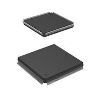
HD6417750RF200DV Renesas Electronics America, HD6417750RF200DV Datasheet - Page 758

HD6417750RF200DV
Manufacturer Part Number
HD6417750RF200DV
Description
MPU 1.5/3.3V 0K I-TEMP PB-FREE 2
Manufacturer
Renesas Electronics America
Series
SuperH® SH7750r
Datasheet
1.D6417750RBP240DV.pdf
(1164 pages)
Specifications of HD6417750RF200DV
Core Processor
SH-4
Core Size
32-Bit
Speed
200MHz
Connectivity
EBI/EMI, FIFO, SCI, SmartCard
Peripherals
DMA, POR, WDT
Number Of I /o
28
Program Memory Type
ROMless
Ram Size
48K x 8
Voltage - Supply (vcc/vdd)
1.35 V ~ 1.6 V
Oscillator Type
External
Operating Temperature
-40°C ~ 85°C
Package / Case
208-QFP Exposed Pad, 208-eQFP, 208-HQFP
Lead Free Status / RoHS Status
Lead free / RoHS Compliant
Eeprom Size
-
Program Memory Size
-
Data Converters
-
Available stocks
Company
Part Number
Manufacturer
Quantity
Price
Company:
Part Number:
HD6417750RF200DV
Manufacturer:
FREESCALE
Quantity:
450
- Current page: 758 of 1164
- Download datasheet (7Mb)
Section 15 Serial Communication Interface (SCI)
ERI interrupts are handled by the CPU. The DMAC transfers read data to memory or another
peripheral module. This bit specifies enabling or disabling of the RXI interrupt.
Bit 7: EIO
0
1
Bits 6 to 4—Reserved: These bits are always read as 0, and should only be written with 0.
Bit 3—Serial Port Clock Port I/O (SPB1IO): Specifies serial port SCK pin input/output. When
the SCK pin is actually set as a port output pin and outputs the value set by the SPB1DT bit, the
C/A bit in SCSMR1 and the CKE1 and CKE0 bits in SCSCR1 should be cleared to 0.
Bit 3: SPB1IO
0
1
Bit 2—Serial Port Clock Port Data (SPB1DT): Specifies the serial port SCK pin input/output
data. Input or output is specified by the SPB1IO bit (see the description of bit 3, SPB1IO, for
details). When output is specified, the value of the SPB1DT bit is output to the SCK pin. The SCK
pin value is read from the SPB1DT bit regardless of the value of the SPB1IO bit. The initial value
of this bit after a power-on or manual reset is undefined.
Bit 2: SPB1DT
0
1
Bit 1—Serial Port Break I/O (SPB0IO): Specifies the serial port TxD pin output condition.
When the TxD pin is actually set as a port output pin and outputs the value set by the SPB0DT bit,
the TE bit in SCSCR1 should be cleared to 0.
Bit 1: SPB0IO
0
1
Bit 0—Serial Port Break Data (SPB0DT): Specifies the serial port RxD pin input data and TxD
pin output data. The TxD pin output condition is specified by the SPB0IO bit (see the description
of bit 1, SPB0IO, for details). When the TxD pin is designated as an output, the value of the
Rev.7.00 Oct. 10, 2008 Page 672 of 1074
REJ09B0366-0700
Description
When the RIE bit is 1, RXI and ERI interrupts are sent to INTC (Initial value)
When the RIE bit is 1, only ERI interrupts are sent to INTC
Description
SPB1DT bit value is not output to the SCK pin
SPB1DT bit value is output to the SCK pin
Description
Input/output data is low-level
Input/output data is high-level
Description
SPB0DT bit value is not output to the TxD pin
SPB0DT bit value is output to the TxD pin
(Initial value)
(Initial value)
Related parts for HD6417750RF200DV
Image
Part Number
Description
Manufacturer
Datasheet
Request
R

Part Number:
Description:
KIT STARTER FOR M16C/29
Manufacturer:
Renesas Electronics America
Datasheet:

Part Number:
Description:
KIT STARTER FOR R8C/2D
Manufacturer:
Renesas Electronics America
Datasheet:

Part Number:
Description:
R0K33062P STARTER KIT
Manufacturer:
Renesas Electronics America
Datasheet:

Part Number:
Description:
KIT STARTER FOR R8C/23 E8A
Manufacturer:
Renesas Electronics America
Datasheet:

Part Number:
Description:
KIT STARTER FOR R8C/25
Manufacturer:
Renesas Electronics America
Datasheet:

Part Number:
Description:
KIT STARTER H8S2456 SHARPE DSPLY
Manufacturer:
Renesas Electronics America
Datasheet:

Part Number:
Description:
KIT STARTER FOR R8C38C
Manufacturer:
Renesas Electronics America
Datasheet:

Part Number:
Description:
KIT STARTER FOR R8C35C
Manufacturer:
Renesas Electronics America
Datasheet:

Part Number:
Description:
KIT STARTER FOR R8CL3AC+LCD APPS
Manufacturer:
Renesas Electronics America
Datasheet:

Part Number:
Description:
KIT STARTER FOR RX610
Manufacturer:
Renesas Electronics America
Datasheet:

Part Number:
Description:
KIT STARTER FOR R32C/118
Manufacturer:
Renesas Electronics America
Datasheet:

Part Number:
Description:
KIT DEV RSK-R8C/26-29
Manufacturer:
Renesas Electronics America
Datasheet:

Part Number:
Description:
KIT STARTER FOR SH7124
Manufacturer:
Renesas Electronics America
Datasheet:

Part Number:
Description:
KIT STARTER FOR H8SX/1622
Manufacturer:
Renesas Electronics America
Datasheet:

Part Number:
Description:
KIT DEV FOR SH7203
Manufacturer:
Renesas Electronics America
Datasheet:


