Z8F1233QH020SG Zilog, Z8F1233QH020SG Datasheet - Page 121
Z8F1233QH020SG
Manufacturer Part Number
Z8F1233QH020SG
Description
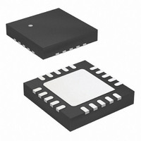
IC ENCORE XP MCU FLSH 12K 20QFN
Manufacturer
Zilog
Series
Encore!®r
Specifications of Z8F1233QH020SG
Core Processor
Z8
Core Size
8-Bit
Speed
20MHz
Peripherals
Brown-out Detect/Reset, LED, POR, PWM, WDT
Number Of I /o
17
Program Memory Size
12KB (12K x 8)
Program Memory Type
FLASH
Ram Size
256 x 8
Voltage - Supply (vcc/vdd)
2.7 V ~ 3.6 V
Oscillator Type
Internal
Operating Temperature
0°C ~ 70°C
Package / Case
20-VQFN Exposed Pad, 20-HVQFN, 20-SQFN, 20-DHVQFN
For Use With
770-1002 - ISP 4PORT ZILOG Z8 ENCORE! MCU
Lead Free Status / RoHS Status
Lead free / RoHS Compliant
Eeprom Size
-
Data Converters
-
Connectivity
-
Other names
269-4656
Available stocks
Company
Part Number
Manufacturer
Quantity
Price
Company:

Part Number:
Z8F1233QH020SG
Manufacturer:
Zilog
Quantity:
670


NVDS Operational Requirements
PS025111-1207
Caution:
Flash Controller Bypass
Flash Controller Behavior in Debug Mode
status register to determine when the Mass Erase operation is complete. When the mass
erase is complete, the Flash controller returns to its Locked state.
The Flash controller can be bypassed and the control signals for the Flash memory are
brought out to the GPIO pins. Bypassing the Flash controller allows faster row
programming algorithms by controlling the Flash programming signals directly.
Row programing is recommended for gang programming applications and large volume
customers who do not require in-circuit initial programming of the Flash memory. Mass
Erase and Page Erase operations are also supported, when the Flash controller is bypassed.
For more information about bypassing the Flash controller, refer to Third-Party Flash
Programming Support for Z8 Encore!
www.zilog.com.
The following behavioral changes can be observed in the Flash controller when the Flash
controller is accessed using the On-Chip Debugger:
•
•
•
•
•
•
•
The device uses a 12 KB Flash memory, despite the maximum specified Flash of 8 KB
size (except 12 KB mode with non-NVDS). User code accesses the lower 8 KB of flash,
leaving the upper 4 K for Zilog memory. The NVDS is implemented by using Zilog
memory for special purpose routines and for the data required by the routines. These
For security reasons, Flash controller allows only a single page to be opened for write/
erase. When writing multiple Flash pages, the Flash controller must go through the
unlock sequence again to select another page.
The Flash write protect option bit is ignored.
The Flash sector protect register is ignored for programming and Erase operations.
Programming operations are not limited to the page selected in the page select register.
Bits in the Flash sector protect register can be written to one or zero.
The second write of the page select register to unlock the flash controller is not
necessary.
The page select register can be written when the Flash controller is unlocked.
The mass erase command is enabled through the Flash control register
®
. This document is available for download at
Z8 Encore!
Product Specification
®
F0830 Series
Flash Memory
111
Related parts for Z8F1233QH020SG
Image
Part Number
Description
Manufacturer
Datasheet
Request
R

Part Number:
Description:
Communication Controllers, ZILOG INTELLIGENT PERIPHERAL CONTROLLER (ZIP)
Manufacturer:
Zilog, Inc.
Datasheet:

Part Number:
Description:
KIT DEV FOR Z8 ENCORE 16K TO 64K
Manufacturer:
Zilog
Datasheet:

Part Number:
Description:
KIT DEV Z8 ENCORE XP 28-PIN
Manufacturer:
Zilog
Datasheet:

Part Number:
Description:
DEV KIT FOR Z8 ENCORE 8K/4K
Manufacturer:
Zilog
Datasheet:

Part Number:
Description:
KIT DEV Z8 ENCORE XP 28-PIN
Manufacturer:
Zilog
Datasheet:

Part Number:
Description:
DEV KIT FOR Z8 ENCORE 4K TO 8K
Manufacturer:
Zilog
Datasheet:
Part Number:
Description:
CMOS Z8 microcontroller. ROM 16 Kbytes, RAM 256 bytes, speed 16 MHz, 32 lines I/O, 3.0V to 5.5V
Manufacturer:
Zilog, Inc.
Datasheet:
Part Number:
Description:
Low-cost microcontroller. 512 bytes ROM, 61 bytes RAM, 8 MHz
Manufacturer:
Zilog, Inc.
Datasheet:
Part Number:
Description:
Z8 4K OTP Microcontroller
Manufacturer:
Zilog, Inc.
Datasheet:
Part Number:
Description:
CMOS SUPER8 ROMLESS MCU
Manufacturer:
Zilog, Inc.
Datasheet:
Part Number:
Description:
SL1866 CMOSZ8 OTP Microcontroller
Manufacturer:
Zilog, Inc.
Datasheet:
Part Number:
Description:
SL1866 CMOSZ8 OTP Microcontroller
Manufacturer:
Zilog, Inc.
Datasheet:
Part Number:
Description:
OTP (KB) = 1, RAM = 125, Speed = 12, I/O = 14, 8-bit Timers = 2, Comm Interfaces Other Features = Por, LV Protect, Voltage = 4.5-5.5V
Manufacturer:
Zilog, Inc.
Datasheet:
Part Number:
Description:
Manufacturer:
Zilog, Inc.
Datasheet: