Z8F1233QH020SG Zilog, Z8F1233QH020SG Datasheet - Page 88
Z8F1233QH020SG
Manufacturer Part Number
Z8F1233QH020SG
Description
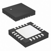
IC ENCORE XP MCU FLSH 12K 20QFN
Manufacturer
Zilog
Series
Encore!®r
Specifications of Z8F1233QH020SG
Core Processor
Z8
Core Size
8-Bit
Speed
20MHz
Peripherals
Brown-out Detect/Reset, LED, POR, PWM, WDT
Number Of I /o
17
Program Memory Size
12KB (12K x 8)
Program Memory Type
FLASH
Ram Size
256 x 8
Voltage - Supply (vcc/vdd)
2.7 V ~ 3.6 V
Oscillator Type
Internal
Operating Temperature
0°C ~ 70°C
Package / Case
20-VQFN Exposed Pad, 20-HVQFN, 20-SQFN, 20-DHVQFN
For Use With
770-1002 - ISP 4PORT ZILOG Z8 ENCORE! MCU
Lead Free Status / RoHS Status
Lead free / RoHS Compliant
Eeprom Size
-
Data Converters
-
Connectivity
-
Other names
269-4656
Available stocks
Company
Part Number
Manufacturer
Quantity
Price
Company:

Part Number:
Z8F1233QH020SG
Manufacturer:
Zilog
Quantity:
670


Table 47. Timer 0–1 High Byte Register (TxH)
Timer Control Register Definitions
BITS
FIELD
RESET
R/W
ADDR
PS025111-1207
Timer Pin Signal Operation
Timer 0–1 High and Low Byte Registers
R/W
0
7
register is read, the contents of the timer low byte register are placed in a holding register.
A subsequent read from the timer low byte register returns the value in the holding
register. This operation allows accurate reads of the full 16-bit timer count value when
enabled. When the timers are not enabled, a read from the timer low byte register returns
the actual value in the counter.
Timer output is a GPIO port pin alternate function. The timer output is toggled every time
the counter is reloaded.
The timer input can be used as a selectable counting source. It shares the same pin as the
complementary timer output. When selected by the GPIO alternate function registers, this
pin functions as a timer input in all modes except for the DUAL PWM OUTPUT mode.
For this mode, no timer input is available.
The Timer 0–1 high and low byte (TxH and TxL) registers
contain the current 16-bit timer count value. When the timer is enabled, a read from TxH
causes the value in TxL to be stored in a temporary holding register. A read from TxL
always returns this temporary register content when the timer is enabled, however, when
the timer is disabled, a read from the TxL reads the TxL register content directly.
Writing to the timer high and low byte registers, while the timer is enabled is not
recommended. There are no temporary holding registers available for Write operations, so
simultaneous 16-bit writes are not possible. If either the timer high or low byte registers
are written during counting, the 8-bit written value is placed in the counter (high or low
byte) at the next clock edge. The counter continues counting from the new value.
R/W
6
0
R/W
5
0
R/W
0
4
F00H, F08H
TH
R/W
3
0
R/W
(Table 47
Z8 Encore!
0
2
Product Specification
and
R/W
1
0
®
Table
F0830 Series
48)
R/W
0
0
Timers
78
Related parts for Z8F1233QH020SG
Image
Part Number
Description
Manufacturer
Datasheet
Request
R

Part Number:
Description:
Communication Controllers, ZILOG INTELLIGENT PERIPHERAL CONTROLLER (ZIP)
Manufacturer:
Zilog, Inc.
Datasheet:

Part Number:
Description:
KIT DEV FOR Z8 ENCORE 16K TO 64K
Manufacturer:
Zilog
Datasheet:

Part Number:
Description:
KIT DEV Z8 ENCORE XP 28-PIN
Manufacturer:
Zilog
Datasheet:

Part Number:
Description:
DEV KIT FOR Z8 ENCORE 8K/4K
Manufacturer:
Zilog
Datasheet:

Part Number:
Description:
KIT DEV Z8 ENCORE XP 28-PIN
Manufacturer:
Zilog
Datasheet:

Part Number:
Description:
DEV KIT FOR Z8 ENCORE 4K TO 8K
Manufacturer:
Zilog
Datasheet:
Part Number:
Description:
CMOS Z8 microcontroller. ROM 16 Kbytes, RAM 256 bytes, speed 16 MHz, 32 lines I/O, 3.0V to 5.5V
Manufacturer:
Zilog, Inc.
Datasheet:
Part Number:
Description:
Low-cost microcontroller. 512 bytes ROM, 61 bytes RAM, 8 MHz
Manufacturer:
Zilog, Inc.
Datasheet:
Part Number:
Description:
Z8 4K OTP Microcontroller
Manufacturer:
Zilog, Inc.
Datasheet:
Part Number:
Description:
CMOS SUPER8 ROMLESS MCU
Manufacturer:
Zilog, Inc.
Datasheet:
Part Number:
Description:
SL1866 CMOSZ8 OTP Microcontroller
Manufacturer:
Zilog, Inc.
Datasheet:
Part Number:
Description:
SL1866 CMOSZ8 OTP Microcontroller
Manufacturer:
Zilog, Inc.
Datasheet:
Part Number:
Description:
OTP (KB) = 1, RAM = 125, Speed = 12, I/O = 14, 8-bit Timers = 2, Comm Interfaces Other Features = Por, LV Protect, Voltage = 4.5-5.5V
Manufacturer:
Zilog, Inc.
Datasheet:
Part Number:
Description:
Manufacturer:
Zilog, Inc.
Datasheet: