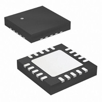
Z8F1233QH020SG Zilog, Z8F1233QH020SG Datasheet - Page 49

Z8F1233QH020SG
Manufacturer Part Number
Z8F1233QH020SG
Description
IC ENCORE XP MCU FLSH 12K 20QFN
Manufacturer
Zilog
Series
Encore!®r
Specifications of Z8F1233QH020SG
Core Processor
Z8
Core Size
8-Bit
Speed
20MHz
Peripherals
Brown-out Detect/Reset, LED, POR, PWM, WDT
Number Of I /o
17
Program Memory Size
12KB (12K x 8)
Program Memory Type
FLASH
Ram Size
256 x 8
Voltage - Supply (vcc/vdd)
2.7 V ~ 3.6 V
Oscillator Type
Internal
Operating Temperature
0°C ~ 70°C
Package / Case
20-VQFN Exposed Pad, 20-HVQFN, 20-SQFN, 20-DHVQFN
For Use With
770-1002 - ISP 4PORT ZILOG Z8 ENCORE! MCU
Lead Free Status / RoHS Status
Lead free / RoHS Compliant
Eeprom Size
-
Data Converters
-
Connectivity
-
Other names
269-4656
Available stocks
Company
Part Number
Manufacturer
Quantity
Price
Company:
Part Number:
Z8F1233QH020SG
Manufacturer:
Zilog
Quantity:
670
- Current page: 49 of 251
- Download datasheet (4Mb)
Direct LED Drive
Shared Reset Pin
Crystal Oscillator Override
5 V Tolerance
External Clock Setup
PS025111-1207
The port C pins provide a sinked current output, capable of driving an LED without
requiring an external resistor. The output sinks current at programmable levels, 3 mA,
7 mA, 13 mA, and 20 mA. This mode is enabled through the Alternate function
sub-register AFS1 and is programmable through the LED control registers.
For proper function, the LED anode must be connected to V
GPIO pin.
Using all Port C pins in LED drive mode with maximum current may result in excessive
total current. See
the applicable package.
On the 20- and 28-pin devices, the port D0 pin shares function with a bidirectional reset
pin. Unlike all other I/O pins, this pin does not default to GPIO function on power-up.
This pin acts as a bidirectional reset until the user software re-configures it. When in GPIO
mode, the port D0 pin functions as output only.
For systems using a crystal oscillator, the pins PA0 and PA1 are connected to the crystal.
When the crystal oscillator is enabled, the GPIO settings are overridden and PA0 and PA1
are disabled. See
In the 20- and 28-pin versions of this device, any pin, which shares functionality with an
ADC, crystal or comparator port is not 5 V tolerant, including PA[1:0], PB[5:0] and
PC[2:0]. All other signal pins are 5 V tolerant, and can safely handle inputs higher than
V
resistor.
For systems using an external TTL drive, PB3 is the clock source for 20- and 28-pin
devices. In this case, configure PB3 for Alternate function CLKIN. Write to the oscillator
DD
even with the pull-ups enabled, but with excess power consumption on pull-up
Oscillator Control Register Definitions
Electrical Characteristics
on page 177 for the maximum total current for
on page 146.
Z8 Encore!
DD
General Purpose Input/Output
and the cathode to the
Product Specification
®
F0830 Series
39
Related parts for Z8F1233QH020SG
Image
Part Number
Description
Manufacturer
Datasheet
Request
R

Part Number:
Description:
Communication Controllers, ZILOG INTELLIGENT PERIPHERAL CONTROLLER (ZIP)
Manufacturer:
Zilog, Inc.
Datasheet:

Part Number:
Description:
KIT DEV FOR Z8 ENCORE 16K TO 64K
Manufacturer:
Zilog
Datasheet:

Part Number:
Description:
KIT DEV Z8 ENCORE XP 28-PIN
Manufacturer:
Zilog
Datasheet:

Part Number:
Description:
DEV KIT FOR Z8 ENCORE 8K/4K
Manufacturer:
Zilog
Datasheet:

Part Number:
Description:
KIT DEV Z8 ENCORE XP 28-PIN
Manufacturer:
Zilog
Datasheet:

Part Number:
Description:
DEV KIT FOR Z8 ENCORE 4K TO 8K
Manufacturer:
Zilog
Datasheet:

Part Number:
Description:
CMOS Z8 microcontroller. ROM 16 Kbytes, RAM 256 bytes, speed 16 MHz, 32 lines I/O, 3.0V to 5.5V
Manufacturer:
Zilog, Inc.
Datasheet:

Part Number:
Description:
Low-cost microcontroller. 512 bytes ROM, 61 bytes RAM, 8 MHz
Manufacturer:
Zilog, Inc.
Datasheet:

Part Number:
Description:
Z8 4K OTP Microcontroller
Manufacturer:
Zilog, Inc.
Datasheet:

Part Number:
Description:
CMOS SUPER8 ROMLESS MCU
Manufacturer:
Zilog, Inc.
Datasheet:

Part Number:
Description:
SL1866 CMOSZ8 OTP Microcontroller
Manufacturer:
Zilog, Inc.
Datasheet:

Part Number:
Description:
SL1866 CMOSZ8 OTP Microcontroller
Manufacturer:
Zilog, Inc.
Datasheet:

Part Number:
Description:
OTP (KB) = 1, RAM = 125, Speed = 12, I/O = 14, 8-bit Timers = 2, Comm Interfaces Other Features = Por, LV Protect, Voltage = 4.5-5.5V
Manufacturer:
Zilog, Inc.
Datasheet:

Part Number:
Description:
Manufacturer:
Zilog, Inc.
Datasheet:


