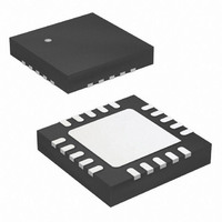
Z8F1233QH020SG Zilog, Z8F1233QH020SG Datasheet - Page 82

Z8F1233QH020SG
Manufacturer Part Number
Z8F1233QH020SG
Description
IC ENCORE XP MCU FLSH 12K 20QFN
Manufacturer
Zilog
Series
Encore!®r
Specifications of Z8F1233QH020SG
Core Processor
Z8
Core Size
8-Bit
Speed
20MHz
Peripherals
Brown-out Detect/Reset, LED, POR, PWM, WDT
Number Of I /o
17
Program Memory Size
12KB (12K x 8)
Program Memory Type
FLASH
Ram Size
256 x 8
Voltage - Supply (vcc/vdd)
2.7 V ~ 3.6 V
Oscillator Type
Internal
Operating Temperature
0°C ~ 70°C
Package / Case
20-VQFN Exposed Pad, 20-HVQFN, 20-SQFN, 20-DHVQFN
For Use With
770-1002 - ISP 4PORT ZILOG Z8 ENCORE! MCU
Lead Free Status / RoHS Status
Lead free / RoHS Compliant
Eeprom Size
-
Data Converters
-
Connectivity
-
Other names
269-4656
Available stocks
Company
Part Number
Manufacturer
Quantity
Price
Company:
Part Number:
Z8F1233QH020SG
Manufacturer:
Zilog
Quantity:
670
- Current page: 82 of 251
- Download datasheet (4Mb)
PS025111-1207
Follow the steps below for configuring a timer for PWM DUAL OUTPUT mode and for
initiating the PWM operation:
1. Write to the timer control register to:
2. Write to the timer high and low byte registers to set the starting count value (typically
3. Write to the PWM high and low byte registers to set the PWM value.
4. Write to the PWM control register to set the PWM deadband delay value. The
5. Write to the timer reload high and low byte registers to set the reload value (PWM
6. If appropriate, enable the timer interrupt and set the timer interrupt priority by writing
7. Configure the associated GPIO port pin for the timer output and timer output
8. Write to the timer control register to enable the timer and initiate counting.
The PWM period is represented by the following equation:
If an initial starting value other than
registers, the ONE-SHOT mode equation determines the first PWM time-out period.
If TPOL is set to 0, the ratio of the PWM output high time to the total period is represented
by:
PWM Output High Time Ratio (%)
PWM Period (s)
–
–
–
–
0001H
PWM mode, counting always begins at the reset value of
deadband delay must be less than the duration of the positive phase of the PWM signal
(as defined by the PWM high and low byte registers). It must also be less than the
duration of the negative phase of the PWM signal (as defined by the difference
between the PWM registers and the timer reload registers).
period). The reload value must be greater than the PWM value.
to the relevant interrupt registers.
complement alternate functions. The timer output complement function is shared with
the timer input function for both timers. Setting the timer mode to dual PWM, will
automatically switch the function from timer-in to timer-out complement.
Disable the timer
Configure the timer for PWM DUAL OUTPUT mode. Setting the mode also
involves writing to TMODEHI bit in TxCTL1 register.
Set the prescale value.
Set the initial logic level (high or low) and PWM high/low transition for the timer
output alternate function.
). This only affects the first pass in PWM mode. After the first timer reset in
=
--------------------------------------------------------------------------- -
System Clock Frequency (Hz)
Reload Value
0001H
=
×
Reload Value PWM Value
----------------------------------------------------------------------- -
Prescale
is loaded into the timer high and low byte
Reload Value
–
Z8 Encore!
0001H
Product Specification
.
®
×
100
F0830 Series
Timers
72
Related parts for Z8F1233QH020SG
Image
Part Number
Description
Manufacturer
Datasheet
Request
R

Part Number:
Description:
Communication Controllers, ZILOG INTELLIGENT PERIPHERAL CONTROLLER (ZIP)
Manufacturer:
Zilog, Inc.
Datasheet:

Part Number:
Description:
KIT DEV FOR Z8 ENCORE 16K TO 64K
Manufacturer:
Zilog
Datasheet:

Part Number:
Description:
KIT DEV Z8 ENCORE XP 28-PIN
Manufacturer:
Zilog
Datasheet:

Part Number:
Description:
DEV KIT FOR Z8 ENCORE 8K/4K
Manufacturer:
Zilog
Datasheet:

Part Number:
Description:
KIT DEV Z8 ENCORE XP 28-PIN
Manufacturer:
Zilog
Datasheet:

Part Number:
Description:
DEV KIT FOR Z8 ENCORE 4K TO 8K
Manufacturer:
Zilog
Datasheet:

Part Number:
Description:
CMOS Z8 microcontroller. ROM 16 Kbytes, RAM 256 bytes, speed 16 MHz, 32 lines I/O, 3.0V to 5.5V
Manufacturer:
Zilog, Inc.
Datasheet:

Part Number:
Description:
Low-cost microcontroller. 512 bytes ROM, 61 bytes RAM, 8 MHz
Manufacturer:
Zilog, Inc.
Datasheet:

Part Number:
Description:
Z8 4K OTP Microcontroller
Manufacturer:
Zilog, Inc.
Datasheet:

Part Number:
Description:
CMOS SUPER8 ROMLESS MCU
Manufacturer:
Zilog, Inc.
Datasheet:

Part Number:
Description:
SL1866 CMOSZ8 OTP Microcontroller
Manufacturer:
Zilog, Inc.
Datasheet:

Part Number:
Description:
SL1866 CMOSZ8 OTP Microcontroller
Manufacturer:
Zilog, Inc.
Datasheet:

Part Number:
Description:
OTP (KB) = 1, RAM = 125, Speed = 12, I/O = 14, 8-bit Timers = 2, Comm Interfaces Other Features = Por, LV Protect, Voltage = 4.5-5.5V
Manufacturer:
Zilog, Inc.
Datasheet:

Part Number:
Description:
Manufacturer:
Zilog, Inc.
Datasheet:


