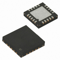
ATTINY4313-MU Atmel, ATTINY4313-MU Datasheet - Page 145

ATTINY4313-MU
Manufacturer Part Number
ATTINY4313-MU
Description
IC MCU AVR 4K FLASH 20QFN
Manufacturer
Atmel
Series
AVR® ATtinyr
Specifications of ATTINY4313-MU
Core Processor
AVR
Core Size
8-Bit
Speed
20MHz
Connectivity
I²C, SPI, UART/USART
Peripherals
Brown-out Detect/Reset, POR, PWM, WDT
Number Of I /o
18
Program Memory Size
4KB (2K x 16)
Program Memory Type
FLASH
Eeprom Size
256 x 8
Ram Size
256 x 8
Voltage - Supply (vcc/vdd)
1.8 V ~ 5.5 V
Oscillator Type
Internal
Operating Temperature
-40°C ~ 85°C
Package / Case
20-VQFN Exposed Pad, 20-HVQFN, 20-SQFN, 20-DHVQFN
Processor Series
ATtiny
Core
AVR
Data Bus Width
8 bit
Data Ram Size
256 B
Interface Type
SPI, USART, USI
Maximum Clock Frequency
20 MHz
Number Of Programmable I/os
18
Number Of Timers
2
Operating Supply Voltage
3.3 V
Maximum Operating Temperature
+ 85 C
Mounting Style
SMD/SMT
Minimum Operating Temperature
- 40 C
Operating Temperature Range
- 40 C to + 85 C
Lead Free Status / RoHS Status
Lead free / RoHS Compliant
Data Converters
-
Lead Free Status / Rohs Status
Details
Available stocks
Company
Part Number
Manufacturer
Quantity
Price
Company:
Part Number:
ATTINY4313-MU
Manufacturer:
HITTITE
Quantity:
101
- Current page: 145 of 270
- Download datasheet (7Mb)
15. USART in SPI Mode
15.1
15.2
15.3
8246A–AVR–11/09
Features
Overview
Clock Generation
•
•
•
•
•
•
•
•
The Universal Synchronous and Asynchronous serial Receiver and Transmitter (USART) can be
set to a master SPI compliant mode of operation.
Setting both UMSEL1:0 bits to one enables the USART in MSPIM logic. In this mode of opera-
tion the SPI master control logic takes direct control over the USART resources. These
resources include the transmitter and receiver shift register and buffers, and the baud rate gen-
erator. The parity generator and checker, the data and clock recovery logic, and the RX and TX
control logic is disabled. The USART RX and TX control logic is replaced by a common SPI
transfer control logic. However, the pin control logic and interrupt generation logic is identical in
both modes of operation.
The I/O register locations are the same in both modes. However, some of the functionality of the
control registers changes when using MSPIM.
The Clock Generation logic generates the base clock for the Transmitter and Receiver. For
USART MSPIM mode of operation only internal clock generation (i.e. master operation) is sup-
ported. The Data Direction Register for the XCK pin (DDR_XCK) must therefore be set to one
(i.e. as output) for the USART in MSPIM to operate correctly. Preferably the DDR_XCK should
be set up before the USART in MSPIM is enabled (i.e. TXEN and RXEN bit set to one).
The internal clock generation used in MSPIM mode is identical to the USART synchronous mas-
ter mode. The baud rate or UBRR setting can therefore be calculated using the same equations,
see
Full Duplex, Three-wire Synchronous Data Transfer
Master Operation
Supports all four SPI Modes of Operation (Mode 0, 1, 2, and 3)
LSB First or MSB First Data Transfer (Configurable Data Order)
Queued Operation (Double Buffered)
High Resolution Baud Rate Generator
High Speed Operation (f
Flexible Interrupt Generation
Table
15-1:
XCKmax
= f
CK
/2)
145
Related parts for ATTINY4313-MU
Image
Part Number
Description
Manufacturer
Datasheet
Request
R

Part Number:
Description:
Manufacturer:
Atmel Corporation
Datasheet:

Part Number:
Description:
Microcontrollers (MCU) 512B FL 32B SRAM TIMER ATTINY4 12MHz
Manufacturer:
Atmel

Part Number:
Description:
IC MCU AVR 512B FLASH SOT-23-6
Manufacturer:
Atmel
Datasheet:

Part Number:
Description:
IC MCU AVR 512B FLASH SOT-23-6
Manufacturer:
Atmel
Datasheet:

Part Number:
Description:
DEV KIT FOR AVR/AVR32
Manufacturer:
Atmel
Datasheet:

Part Number:
Description:
INTERVAL AND WIPE/WASH WIPER CONTROL IC WITH DELAY
Manufacturer:
ATMEL Corporation
Datasheet:

Part Number:
Description:
Low-Voltage Voice-Switched IC for Hands-Free Operation
Manufacturer:
ATMEL Corporation
Datasheet:

Part Number:
Description:
MONOLITHIC INTEGRATED FEATUREPHONE CIRCUIT
Manufacturer:
ATMEL Corporation
Datasheet:

Part Number:
Description:
AM-FM Receiver IC U4255BM-M
Manufacturer:
ATMEL Corporation
Datasheet:

Part Number:
Description:
Monolithic Integrated Feature Phone Circuit
Manufacturer:
ATMEL Corporation
Datasheet:

Part Number:
Description:
Multistandard Video-IF and Quasi Parallel Sound Processing
Manufacturer:
ATMEL Corporation
Datasheet:


