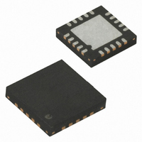
ATTINY4313-MU Atmel, ATTINY4313-MU Datasheet - Page 62

ATTINY4313-MU
Manufacturer Part Number
ATTINY4313-MU
Description
IC MCU AVR 4K FLASH 20QFN
Manufacturer
Atmel
Series
AVR® ATtinyr
Specifications of ATTINY4313-MU
Core Processor
AVR
Core Size
8-Bit
Speed
20MHz
Connectivity
I²C, SPI, UART/USART
Peripherals
Brown-out Detect/Reset, POR, PWM, WDT
Number Of I /o
18
Program Memory Size
4KB (2K x 16)
Program Memory Type
FLASH
Eeprom Size
256 x 8
Ram Size
256 x 8
Voltage - Supply (vcc/vdd)
1.8 V ~ 5.5 V
Oscillator Type
Internal
Operating Temperature
-40°C ~ 85°C
Package / Case
20-VQFN Exposed Pad, 20-HVQFN, 20-SQFN, 20-DHVQFN
Processor Series
ATtiny
Core
AVR
Data Bus Width
8 bit
Data Ram Size
256 B
Interface Type
SPI, USART, USI
Maximum Clock Frequency
20 MHz
Number Of Programmable I/os
18
Number Of Timers
2
Operating Supply Voltage
3.3 V
Maximum Operating Temperature
+ 85 C
Mounting Style
SMD/SMT
Minimum Operating Temperature
- 40 C
Operating Temperature Range
- 40 C to + 85 C
Lead Free Status / RoHS Status
Lead free / RoHS Compliant
Data Converters
-
Lead Free Status / Rohs Status
Details
Available stocks
Company
Part Number
Manufacturer
Quantity
Price
Company:
Part Number:
ATTINY4313-MU
Manufacturer:
HITTITE
Quantity:
101
- Current page: 62 of 270
- Download datasheet (7Mb)
10.2.2
62
ATtiny2313A/4313
Alternate Functions of Port B
Table 10-4
5 on page
Table 10-4.
Notes:
The Port B pins with alternate function are shown in
Table 10-5.
Signal
Name
PUOE
PUOV
DDOE
DDOV
PVOE
PVOV
PTOE
DIEOE
DIEOV
DI
AIO
1. RSTDISBL is 1 when the fuse is “0” (Programmed).
2. DebugWIRE is enabled when DWEN Fuse is programmed and Lock bits are unprogrammed.
3. EXT_OSC = crystal oscillator or low frequency crystal oscillator is selected as system clock.
4. EXT_CLOCK = external closk is selected as system clock.
Port Pin
59.
PA2/RESET/dW/PCINT10
RSTDISBL
DEBUGWIRE_ENABLE
1
RSTDISBL
DEBUGWIRE_ENABLE
DEBUGWIRE_ENABLE
• debugWire Transmit
RSTDISBL
DEBUGWIRE_ENABLE
0
0
RSTDISBL
DEBUGWIRE_ENABLE
+ PCINT10 • PCIE1
DEBUGWIRE_ENABLE
+ (RSTDISBL
• PCIE1)
dW/PCINT10 Input
relates the alternate functions of Port A to the overriding signals shown in
PB0
PB1
PB2
PB3
Overriding Signals for Alternate Functions in PA2..PA0
Port B Pins Alternate Functions
(1)
(1)
(1)
(1)
+
+
+
+
(1)
• PCINT10
Alternate Function
AIN0:
PCINT0:Pin Change Interrupt 0, Source 0
AIN1:
PCINT1: Pin Change Interrupt 0, Source 1
OC0A:: Timer/Counter0 Compare Match AOutput
PCINT2: Pin Change Interrupt 0, Source 2
OC1A: Timer/Counter1 Compare Match A Output
PCINT3: Pin Change Interrupt 0, Source 3
(2)
(2)
(2)
(2)
(2)
(2)
Analog Comparator, Positive Input
Analog Comparator, Negative Input
EXT_OSC
0
EXT_OSC
0
EXT_OSC
0
0
EXT_OSC
• PCIE1
EXT_OSC
• PCIE1
PCINT9 Input
XTAL2
PA1/XTAL2/PCINT9
(3)
(3)
(3)
(3)
(3)
+ PCINT9
+ PCINT9
Table
10-5.
PA0/XTAL1/PCINT8
EXT_CLOCK
0
EXT_CLOCK
0
EXT_CLOCK
0
0
EXT_CLOCK
+ (PCINT8 • PCIE1)
(EXT_CLOCK
(EXT_CLOCK
PCINT8 • PCIE1)
CLKI/PCINT8 Input
XTAL1
(4)
(4)
(4)
(4)
(4)
(4)
+ EXT_OSC
+ EXT_OSC
+ EXT_OSC
+ EXT_OSC
• PWR_DOWN) +
• EXT_OSC
8246A–AVR–11/09
Figure 10-
(3)
(3)
(3)
(3)
(3)
•
Related parts for ATTINY4313-MU
Image
Part Number
Description
Manufacturer
Datasheet
Request
R

Part Number:
Description:
Manufacturer:
Atmel Corporation
Datasheet:

Part Number:
Description:
Microcontrollers (MCU) 512B FL 32B SRAM TIMER ATTINY4 12MHz
Manufacturer:
Atmel

Part Number:
Description:
IC MCU AVR 512B FLASH SOT-23-6
Manufacturer:
Atmel
Datasheet:

Part Number:
Description:
IC MCU AVR 512B FLASH SOT-23-6
Manufacturer:
Atmel
Datasheet:

Part Number:
Description:
DEV KIT FOR AVR/AVR32
Manufacturer:
Atmel
Datasheet:

Part Number:
Description:
INTERVAL AND WIPE/WASH WIPER CONTROL IC WITH DELAY
Manufacturer:
ATMEL Corporation
Datasheet:

Part Number:
Description:
Low-Voltage Voice-Switched IC for Hands-Free Operation
Manufacturer:
ATMEL Corporation
Datasheet:

Part Number:
Description:
MONOLITHIC INTEGRATED FEATUREPHONE CIRCUIT
Manufacturer:
ATMEL Corporation
Datasheet:

Part Number:
Description:
AM-FM Receiver IC U4255BM-M
Manufacturer:
ATMEL Corporation
Datasheet:

Part Number:
Description:
Monolithic Integrated Feature Phone Circuit
Manufacturer:
ATMEL Corporation
Datasheet:

Part Number:
Description:
Multistandard Video-IF and Quasi Parallel Sound Processing
Manufacturer:
ATMEL Corporation
Datasheet:


