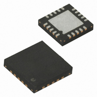
ATTINY4313-MU Atmel, ATTINY4313-MU Datasheet - Page 67

ATTINY4313-MU
Manufacturer Part Number
ATTINY4313-MU
Description
IC MCU AVR 4K FLASH 20QFN
Manufacturer
Atmel
Series
AVR® ATtinyr
Specifications of ATTINY4313-MU
Core Processor
AVR
Core Size
8-Bit
Speed
20MHz
Connectivity
I²C, SPI, UART/USART
Peripherals
Brown-out Detect/Reset, POR, PWM, WDT
Number Of I /o
18
Program Memory Size
4KB (2K x 16)
Program Memory Type
FLASH
Eeprom Size
256 x 8
Ram Size
256 x 8
Voltage - Supply (vcc/vdd)
1.8 V ~ 5.5 V
Oscillator Type
Internal
Operating Temperature
-40°C ~ 85°C
Package / Case
20-VQFN Exposed Pad, 20-HVQFN, 20-SQFN, 20-DHVQFN
Processor Series
ATtiny
Core
AVR
Data Bus Width
8 bit
Data Ram Size
256 B
Interface Type
SPI, USART, USI
Maximum Clock Frequency
20 MHz
Number Of Programmable I/os
18
Number Of Timers
2
Operating Supply Voltage
3.3 V
Maximum Operating Temperature
+ 85 C
Mounting Style
SMD/SMT
Minimum Operating Temperature
- 40 C
Operating Temperature Range
- 40 C to + 85 C
Lead Free Status / RoHS Status
Lead free / RoHS Compliant
Data Converters
-
Lead Free Status / Rohs Status
Details
Available stocks
Company
Part Number
Manufacturer
Quantity
Price
Company:
Part Number:
ATTINY4313-MU
Manufacturer:
HITTITE
Quantity:
101
- Current page: 67 of 270
- Download datasheet (7Mb)
8246A–AVR–11/09
• Port D, Bit 4 – T0/PCINT15
• Port D, Bit 5 – OC0B/T1/PCINT16
• Port D, Bit 6 – ICPI/PCINT17
Table 10-9
shown in
Table 10-9.
Signal
Name
PUOE
PUOV
DDOE
DDOV
PVOE
PVOV
PTOE
DIEOE
DIEOV
DI
AIO
• T0: Timer/Counter0 External Counter Clock input is enabled by setting (one) the bits CS02
• PCINT15: Pin Change Interrupt Source 15. The PD4 pin can serve as an external interrupt
• OC0B: Output Compare Match B output: The PD5 pin can serve as an external output for the
• T1: Timer/Counter1 External Counter Clock input is enabled by setting (one) the bits CS02
• PCINT16: Pin Change Interrupt Source 16. The PD5 pin can serve as an external interrupt
• ICPI: Timer/Counter1 Input Capture Pin. The PD6 pin can act as an Input Capture pin for
• PCINT17: Pin Change Interrupt Source 17. The PD6 pin can serve as an external interrupt
and CS01 in the Timer/Counter0 Control Register (TCCR0).
source for pin change interrupt 2.
Timer/Counter0 Output Compare B. The pin has to be configured as an output (DDD5 set
(one)) to serve this function. The OC0B pin is also the output pin for the PWM mode timer
function.
and CS01 in the Timer/Counter1 Control Register (TCCR1).
source for pin change interrupt 2.
Timer/Counter1.
source for pin change interrupt 2.
Figure 10-5 on page
PD6/ICPI/PCINT17
0
0
0
0
0
0
0
ICPI Enable + PCINT17
PCINT17
ICPI Input/PCINT17
–
and
Overriding Signals for Alternate Functions PD6..PD4
Table 10-10
relates the alternate functions of Port D to the overriding signals
59.
T1 Enable + PCINT16
PD5/OC1B/T1/PCINT16
0
0
0
0
OC1B_PVOE
OC1B_PVOV
0
PCINT16
T1 Input/PCINT16
–
T0 Enable + PCINT15
PD4/T0/PCINT15
0
0
0
0
0
0
0
PCINT15
T0 Input/PCINT15
AIN1
67
Related parts for ATTINY4313-MU
Image
Part Number
Description
Manufacturer
Datasheet
Request
R

Part Number:
Description:
Manufacturer:
Atmel Corporation
Datasheet:

Part Number:
Description:
Microcontrollers (MCU) 512B FL 32B SRAM TIMER ATTINY4 12MHz
Manufacturer:
Atmel

Part Number:
Description:
IC MCU AVR 512B FLASH SOT-23-6
Manufacturer:
Atmel
Datasheet:

Part Number:
Description:
IC MCU AVR 512B FLASH SOT-23-6
Manufacturer:
Atmel
Datasheet:

Part Number:
Description:
DEV KIT FOR AVR/AVR32
Manufacturer:
Atmel
Datasheet:

Part Number:
Description:
INTERVAL AND WIPE/WASH WIPER CONTROL IC WITH DELAY
Manufacturer:
ATMEL Corporation
Datasheet:

Part Number:
Description:
Low-Voltage Voice-Switched IC for Hands-Free Operation
Manufacturer:
ATMEL Corporation
Datasheet:

Part Number:
Description:
MONOLITHIC INTEGRATED FEATUREPHONE CIRCUIT
Manufacturer:
ATMEL Corporation
Datasheet:

Part Number:
Description:
AM-FM Receiver IC U4255BM-M
Manufacturer:
ATMEL Corporation
Datasheet:

Part Number:
Description:
Monolithic Integrated Feature Phone Circuit
Manufacturer:
ATMEL Corporation
Datasheet:

Part Number:
Description:
Multistandard Video-IF and Quasi Parallel Sound Processing
Manufacturer:
ATMEL Corporation
Datasheet:


