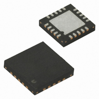
ATTINY4313-MU Atmel, ATTINY4313-MU Datasheet - Page 52

ATTINY4313-MU
Manufacturer Part Number
ATTINY4313-MU
Description
IC MCU AVR 4K FLASH 20QFN
Manufacturer
Atmel
Series
AVR® ATtinyr
Specifications of ATTINY4313-MU
Core Processor
AVR
Core Size
8-Bit
Speed
20MHz
Connectivity
I²C, SPI, UART/USART
Peripherals
Brown-out Detect/Reset, POR, PWM, WDT
Number Of I /o
18
Program Memory Size
4KB (2K x 16)
Program Memory Type
FLASH
Eeprom Size
256 x 8
Ram Size
256 x 8
Voltage - Supply (vcc/vdd)
1.8 V ~ 5.5 V
Oscillator Type
Internal
Operating Temperature
-40°C ~ 85°C
Package / Case
20-VQFN Exposed Pad, 20-HVQFN, 20-SQFN, 20-DHVQFN
Processor Series
ATtiny
Core
AVR
Data Bus Width
8 bit
Data Ram Size
256 B
Interface Type
SPI, USART, USI
Maximum Clock Frequency
20 MHz
Number Of Programmable I/os
18
Number Of Timers
2
Operating Supply Voltage
3.3 V
Maximum Operating Temperature
+ 85 C
Mounting Style
SMD/SMT
Minimum Operating Temperature
- 40 C
Operating Temperature Range
- 40 C to + 85 C
Lead Free Status / RoHS Status
Lead free / RoHS Compliant
Data Converters
-
Lead Free Status / Rohs Status
Details
Available stocks
Company
Part Number
Manufacturer
Quantity
Price
Company:
Part Number:
ATTINY4313-MU
Manufacturer:
HITTITE
Quantity:
101
- Current page: 52 of 270
- Download datasheet (7Mb)
9.3.4
9.3.5
52
ATtiny2313A/4313
PCMSK2 – Pin Change Mask Register 2
PCMSK1 – Pin Change Mask Register 1
Alternatively, the flag can be cleared by writing a logical one to it. This flag is always cleared
when INT1 is configured as a level interrupt.
• Bit 6 – INTF0: External Interrupt Flag 0
When an edge or logic change on the INT0 pin triggers an interrupt request, INTF0 becomes set
(one). If the I-bit in SREG and the INT0 bit in GIMSK are set (one), the MCU will jump to the cor-
responding Interrupt Vector. The flag is cleared when the interrupt routine is executed.
Alternatively, the flag can be cleared by writing a logical one to it. This flag is always cleared
when INT0 is configured as a level interrupt.
• Bit 5 – PCIF0: Pin Change Interrupt Flag 0
When a logic change on any PCINT7..0 pin triggers an interrupt request, PCIF becomes set
(one). If the I-bit in SREG and the PCIE0 bit in GIMSK are set (one), the MCU will jump to the
corresponding Interrupt Vector. The flag is cleared when the interrupt routine is executed. Alter-
natively, the flag can be cleared by writing a logical one to it.
• Bit 4 – PCIF2: Pin Change Interrupt Flag 2
When a logic change on any PCINT17..11 pin triggers an interrupt request, PCIF2 becomes set
(one). If the I-bit in SREG and the PCIE2 bit in GIMSK are set (one), the MCU will jump to the
corresponding Interrupt Vector. The flag is cleared when the interrupt routine is executed. Alter-
natively, the flag can be cleared by writing a logical one to it.
• Bit 3 – PCIF1: Pin Change Interrupt Flag 1
When a logic change on any PCINT10..8 pin triggers an interrupt request, PCIF1 becomes set
(one). If the I-bit in SREG and the PCIE1 bit in GIMSK are set (one), the MCU will jump to the
corresponding Interrupt Vector. The flag is cleared when the interrupt routine is executed. Alter-
natively, the flag can be cleared by writing a logical one to it.
• Bit 7 – Res: Reserved Bit
These bits are reserved and will always read as zero.
• Bits 6..0 – PCINT17..11: Pin Change Enable Mask 17..11
Each PCINT17..11 bit selects whether pin change interrupt is enabled on the corresponding I/O
pin. If PCINT17..11 is set and the PCIE1 bit in GIMSK is set, pin change interrupt is enabled on
the corresponding I/O pin. If PCINT17..11 is cleared, pin change interrupt on the corresponding
I/O pin is disabled.
Bit
0x05 (0x25)
Read/Write
Initial Value
Bit
0x04 (0x24)
Read/Write
Initial Value
R
7
–
0
R
7
–
0
PCINT17
R/W
6
0
R
6
–
0
PCINT16
R/W
5
0
R
5
–
0
PCINT15
R/W
4
0
R
4
–
0
PCINT14
R/W
3
0
3
–
R
0
PCINT13
PCINT10
R/W
R/W
2
0
2
0
PCINT12
PCINT9
R/W
R/W
1
0
1
0
PCINT11
PCINT8
R/W
R/W
0
0
0
0
8246A–AVR–11/09
PCMSK2
PCMSK1
Related parts for ATTINY4313-MU
Image
Part Number
Description
Manufacturer
Datasheet
Request
R

Part Number:
Description:
Manufacturer:
Atmel Corporation
Datasheet:

Part Number:
Description:
Microcontrollers (MCU) 512B FL 32B SRAM TIMER ATTINY4 12MHz
Manufacturer:
Atmel

Part Number:
Description:
IC MCU AVR 512B FLASH SOT-23-6
Manufacturer:
Atmel
Datasheet:

Part Number:
Description:
IC MCU AVR 512B FLASH SOT-23-6
Manufacturer:
Atmel
Datasheet:

Part Number:
Description:
DEV KIT FOR AVR/AVR32
Manufacturer:
Atmel
Datasheet:

Part Number:
Description:
INTERVAL AND WIPE/WASH WIPER CONTROL IC WITH DELAY
Manufacturer:
ATMEL Corporation
Datasheet:

Part Number:
Description:
Low-Voltage Voice-Switched IC for Hands-Free Operation
Manufacturer:
ATMEL Corporation
Datasheet:

Part Number:
Description:
MONOLITHIC INTEGRATED FEATUREPHONE CIRCUIT
Manufacturer:
ATMEL Corporation
Datasheet:

Part Number:
Description:
AM-FM Receiver IC U4255BM-M
Manufacturer:
ATMEL Corporation
Datasheet:

Part Number:
Description:
Monolithic Integrated Feature Phone Circuit
Manufacturer:
ATMEL Corporation
Datasheet:

Part Number:
Description:
Multistandard Video-IF and Quasi Parallel Sound Processing
Manufacturer:
ATMEL Corporation
Datasheet:


