PIC17LC756A-08/L Microchip Technology, PIC17LC756A-08/L Datasheet - Page 108
PIC17LC756A-08/L
Manufacturer Part Number
PIC17LC756A-08/L
Description
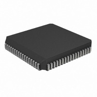
IC MCU OTP 16KX16 A/D 68PLCC
Manufacturer
Microchip Technology
Series
PIC® 17Cr
Specifications of PIC17LC756A-08/L
Core Processor
PIC
Core Size
8-Bit
Speed
8MHz
Connectivity
I²C, SPI, UART/USART
Peripherals
Brown-out Detect/Reset, POR, PWM, WDT
Number Of I /o
50
Program Memory Size
32KB (16K x 16)
Program Memory Type
OTP
Ram Size
902 x 8
Voltage - Supply (vcc/vdd)
3 V ~ 5.5 V
Data Converters
A/D 12x10b
Oscillator Type
External
Operating Temperature
0°C ~ 70°C
Package / Case
68-PLCC
Processor Series
PIC17LC
Core
PIC
Data Bus Width
8 bit
Data Ram Size
902 B
Interface Type
I2C, MSSP, RS- 232, SCI, SPI, USART
Maximum Clock Frequency
8 MHz
Number Of Programmable I/os
50
Number Of Timers
8
Operating Supply Voltage
3 V to 5.5 V
Maximum Operating Temperature
+ 70 C
Mounting Style
SMD/SMT
Minimum Operating Temperature
0 C
On-chip Adc
12 bit
Lead Free Status / RoHS Status
Lead free / RoHS Compliant
Eeprom Size
-
Lead Free Status / Rohs Status
Details
Available stocks
Company
Part Number
Manufacturer
Quantity
Price
Company:

Part Number:
PIC17LC756A-08/L
Manufacturer:
MICROCHIP
Quantity:
12 000
Company:
Part Number:
PIC17LC756A-08/L
Manufacturer:
Microchip Technology
Quantity:
10 000


PIC17C7XX
13.1.3.1
The period of the PWM1 output is determined by
Timer1 and its period register (PR1). The period of the
PWM2 and PWM3 outputs can be individually software
configured to use either Timer1 or Timer2 as the time-
base. For PWM2, when TM2PW2 bit (PW2DCL<5>) is
clear, the time base is determined by TMR1 and PR1
and when TM2PW2 is set, the time base is determined
by Timer2 and PR2. For PWM3, when TM2PW3 bit
(PW3DCL<5>) is clear, the time base is determined by
TMR1 and PR1, and when TM2PW3 is set, the time
base is determined by Timer2 and PR2.
Running two different PWM outputs on two different
timers allows different PWM periods. Running all
PWMs from Timer1 allows the best use of resources by
freeing Timer2 to operate as an 8-bit timer. Timer1 and
Timer2 cannot be used as a 16-bit timer if any PWM is
being used.
The PWM periods can be calculated as follows:
The duty cycle of PWMx is determined by the 10-bit
value DCx<9:0>. The upper 8-bits are from register
PWxDCH and the lower 2-bits are from PWxDCL<7:6>
(PWxDCH:PWxDCL<7:6>). Table 13-4 shows the
maximum PWM frequency (F
the period register.
The number of bits of resolution that the PWM can
achieve depends on the operation frequency of the
device as well as the PWM frequency (F
Maximum PWM resolution (bits) for a given PWM
frequency:
where: F
The PWMx duty cycle is as follows:
where
PWxDCH:PWxDCL.
DS30289B-page 108
period of PWM1 = [(PR1) + 1] x 4T
period of PWM2 = [(PR1) + 1] x 4T
period of PWM3 = [(PR1) + 1] x 4T
PWMx Duty Cycle = (DCx) x T
DCx
PWM
PWM Periods
= 1 / period of PWM
=
represents
log
log (2)
(
[(PR2) + 1] x 4T
[(PR2) + 1] x 4T
F
F
PWM
OSC
the
PWM
)
10-bit
), given the value in
OSC
bits
OSC
OSC
OSC
OSC
OSC
PWM
value
or
or
).
from
If DCx = 0, then the duty cycle is zero. If
PRx = PWxDCH, then the PWM output will be low for
one to four Q-clocks (depending on the state of the
PWxDCL<7:6> bits). For a duty cycle to be 100%, the
PWxDCH value must be greater then the PRx value.
The duty cycle registers for both PWM outputs are dou-
ble buffered. When the user writes to these registers,
they are stored in master latches. When TMR1 (or
TMR2) overflows and a new PWM period begins, the
master latch values are transferred to the slave latches
and the PWMx pin is forced high.
The user should also avoid any "read-modify-write"
operations on the duty cycle registers, such as:
ADDWF PW1DCH. This may cause duty cycle outputs
that are unpredictable.
TABLE 13-4:
13.1.3.2
The PWM modules make use of the TMR1 and/or
TMR2 interrupts. A timer interrupt is generated when
TMR1 or TMR2 equals its period register and on the
following increment is cleared to zero. This interrupt
also marks the beginning of a PWM cycle. The user
can write new duty cycle values before the timer
rollover. The TMR1 interrupt is latched into the TMR1IF
bit and the TMR2 interrupt is latched into the TMR2IF
bit. These flags must be cleared in software.
PRx Value
High
Resolution
Standard
Resolution
Frequency
Note:
PWM
For
PW2DCL, PW3DCH and PW3DCL regis-
ters, a write operation writes to the "master
latches", while a read operation reads the
"slave latches". As a result, the user may
not read back what was just written to the
duty cycle registers (until transferred to
slave latch).
PWM INTERRUPTS
10-bit
0xFF
32.2
8-bit
PW1DCH,
PWM FREQUENCY vs.
RESOLUTION AT 33 MHz
0x7F
64.5
9-bit
7-bit
Frequency (kHz)
2000 Microchip Technology Inc.
8.5-bit
6.5-bit
90.66
PW1DCL,
0x5A
128.9
0x3F
8-bit
6-bit
PW2DCH,
515.6
0x0F
6-bit
4-bit
Related parts for PIC17LC756A-08/L
Image
Part Number
Description
Manufacturer
Datasheet
Request
R

Part Number:
Description:
MICRO CTRL 16K LOW PWR 68PLCC
Manufacturer:
Microchip Technology
Datasheet:
Part Number:
Description:
MICRO CTRL 16K LOW PWR 64SDIP
Manufacturer:
Microchip Technology
Datasheet:
Part Number:
Description:
MICRO CTRL 16K LOW PWR 64SDIP
Manufacturer:
Microchip Technology
Datasheet:
Part Number:
Description:
MICRO CTRL 16K LOW PWR 68PLCC
Manufacturer:
Microchip Technology
Datasheet:

Part Number:
Description:
Manufacturer:
Microchip Technology Inc.
Datasheet:
Part Number:
Description:
Manufacturer:
Microchip Technology Inc.
Datasheet:
Part Number:
Description:
Manufacturer:
Microchip Technology Inc.
Datasheet:
Part Number:
Description:
Manufacturer:
Microchip Technology Inc.
Datasheet:
Part Number:
Description:
Manufacturer:
Microchip Technology Inc.
Datasheet:
Part Number:
Description:
Manufacturer:
Microchip Technology Inc.
Datasheet:
Part Number:
Description:
Manufacturer:
Microchip Technology Inc.
Datasheet: