PIC17LC756A-08/L Microchip Technology, PIC17LC756A-08/L Datasheet - Page 73
PIC17LC756A-08/L
Manufacturer Part Number
PIC17LC756A-08/L
Description
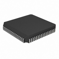
IC MCU OTP 16KX16 A/D 68PLCC
Manufacturer
Microchip Technology
Series
PIC® 17Cr
Specifications of PIC17LC756A-08/L
Core Processor
PIC
Core Size
8-Bit
Speed
8MHz
Connectivity
I²C, SPI, UART/USART
Peripherals
Brown-out Detect/Reset, POR, PWM, WDT
Number Of I /o
50
Program Memory Size
32KB (16K x 16)
Program Memory Type
OTP
Ram Size
902 x 8
Voltage - Supply (vcc/vdd)
3 V ~ 5.5 V
Data Converters
A/D 12x10b
Oscillator Type
External
Operating Temperature
0°C ~ 70°C
Package / Case
68-PLCC
Processor Series
PIC17LC
Core
PIC
Data Bus Width
8 bit
Data Ram Size
902 B
Interface Type
I2C, MSSP, RS- 232, SCI, SPI, USART
Maximum Clock Frequency
8 MHz
Number Of Programmable I/os
50
Number Of Timers
8
Operating Supply Voltage
3 V to 5.5 V
Maximum Operating Temperature
+ 70 C
Mounting Style
SMD/SMT
Minimum Operating Temperature
0 C
On-chip Adc
12 bit
Lead Free Status / RoHS Status
Lead free / RoHS Compliant
Eeprom Size
-
Lead Free Status / Rohs Status
Details
Available stocks
Company
Part Number
Manufacturer
Quantity
Price
Company:

Part Number:
PIC17LC756A-08/L
Manufacturer:
MICROCHIP
Quantity:
12 000
Company:
Part Number:
PIC17LC756A-08/L
Manufacturer:
Microchip Technology
Quantity:
10 000


FIGURE 10-3:
TABLE 10-1:
TABLE 10-2:
RA0/INT
RA1/T0CKI
RA2/SS/SCL
RA3/SDI/SDA
RA4/RX1/DT1
RA5/TX1/CK1
RBPU
Legend: ST = Schmitt Trigger input
10h, Bank 0
05h, Unbanked
13h, Bank 0
15h, Bank 0
Legend: x = unknown, u = unchanged, - = unimplemented, reads as '0'. Shaded cells are not used by PORTA.
Note 1: On any device RESET, these pins are configured as inputs.
2000 Microchip Technology Inc.
Address
Note: I/O pin has protection diodes to V
Name
PORTA
T0STA
RCSTA1
TXSTA1
Name
PORTA FUNCTIONS
REGISTERS/BITS ASSOCIATED WITH PORTA
Bit0
bit0
bit1
bit2
bit3
bit4
bit5
bit7
(1)
D
RA3 BLOCK DIAGRAM
Q
Q
EN
INTEDG
RBPU
CSRC
Buffer Type
SPEN
Bit 7
’1’
Q
CK
Peripheral Data In
ST
ST
ST
ST
ST
ST
—
D
T0SE
Bit 6
RX9
TX9
—
SSP Mode
SS
Input or external interrupt input.
Input or clock input to the TMR0 timer/counter and/or an external interrupt
input.
Input/output or slave select input for the SPI, or clock input for the I
Output is open drain type.
Input/output or data input for the SPI, or data for the I
Output is open drain type.
Input or USART1 Asynchronous Receive input, or
USART1 Synchronous Data input/output.
Input or USART1 Asynchronous Transmit output, or
USART1 Synchronous Clock input/output.
Control bit for PORTB weak pull-ups.
TX1/CK1
WR_PORTA
SDA Out
SREN
TXEN
T0CS
.
Bit 5
RA5/
RD_PORTA
Data Bus
(Q4)
(Q2)
RX1/DT1
T0PS3
CREN
SYNC
Bit 4
RA4/
SDI/SDA
T0PS2
RA3/
Bit 3
—
—
FIGURE 10-4:
Note: I/O pins have protection diodes to V
SS/SCL
T0PS1
FERR
RA2/
Bit 2
OE = SPEN,SYNC,TXEN, CREN, SREN for RA4
OE = SPEN (SYNC+SYNC, CSRC) for RA5
—
Function
RA1/T0CKI
T0PS0
OERR
TRMT
Bit 1
RA4 AND RA5 BLOCK
DIAGRAM
RA0/INT
PIC17C7XX
RX9D
TX9D
Bit 0
—
Serial Port Output Signals
2
Serial Port Input Signal
C bus.
0-xx 11xx
0000 000-
0000 -00x
0000 --1x
Value on
POR,
BOR
DS30289B-page 73
DD
RD_PORTA
and V
2
Data Bus
C bus.
MCLR, WDT
0-uu 11uu
0000 000-
0000 -00u
0000 --1u
SS
(Q2)
.
Related parts for PIC17LC756A-08/L
Image
Part Number
Description
Manufacturer
Datasheet
Request
R

Part Number:
Description:
MICRO CTRL 16K LOW PWR 68PLCC
Manufacturer:
Microchip Technology
Datasheet:
Part Number:
Description:
MICRO CTRL 16K LOW PWR 64SDIP
Manufacturer:
Microchip Technology
Datasheet:
Part Number:
Description:
MICRO CTRL 16K LOW PWR 64SDIP
Manufacturer:
Microchip Technology
Datasheet:
Part Number:
Description:
MICRO CTRL 16K LOW PWR 68PLCC
Manufacturer:
Microchip Technology
Datasheet:

Part Number:
Description:
Manufacturer:
Microchip Technology Inc.
Datasheet:
Part Number:
Description:
Manufacturer:
Microchip Technology Inc.
Datasheet:
Part Number:
Description:
Manufacturer:
Microchip Technology Inc.
Datasheet:
Part Number:
Description:
Manufacturer:
Microchip Technology Inc.
Datasheet:
Part Number:
Description:
Manufacturer:
Microchip Technology Inc.
Datasheet:
Part Number:
Description:
Manufacturer:
Microchip Technology Inc.
Datasheet:
Part Number:
Description:
Manufacturer:
Microchip Technology Inc.
Datasheet: