PIC17LC756A-08/L Microchip Technology, PIC17LC756A-08/L Datasheet - Page 137
PIC17LC756A-08/L
Manufacturer Part Number
PIC17LC756A-08/L
Description
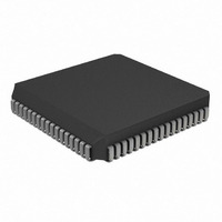
IC MCU OTP 16KX16 A/D 68PLCC
Manufacturer
Microchip Technology
Series
PIC® 17Cr
Specifications of PIC17LC756A-08/L
Core Processor
PIC
Core Size
8-Bit
Speed
8MHz
Connectivity
I²C, SPI, UART/USART
Peripherals
Brown-out Detect/Reset, POR, PWM, WDT
Number Of I /o
50
Program Memory Size
32KB (16K x 16)
Program Memory Type
OTP
Ram Size
902 x 8
Voltage - Supply (vcc/vdd)
3 V ~ 5.5 V
Data Converters
A/D 12x10b
Oscillator Type
External
Operating Temperature
0°C ~ 70°C
Package / Case
68-PLCC
Processor Series
PIC17LC
Core
PIC
Data Bus Width
8 bit
Data Ram Size
902 B
Interface Type
I2C, MSSP, RS- 232, SCI, SPI, USART
Maximum Clock Frequency
8 MHz
Number Of Programmable I/os
50
Number Of Timers
8
Operating Supply Voltage
3 V to 5.5 V
Maximum Operating Temperature
+ 70 C
Mounting Style
SMD/SMT
Minimum Operating Temperature
0 C
On-chip Adc
12 bit
Lead Free Status / RoHS Status
Lead free / RoHS Compliant
Eeprom Size
-
Lead Free Status / Rohs Status
Details
Available stocks
Company
Part Number
Manufacturer
Quantity
Price
Company:

Part Number:
PIC17LC756A-08/L
Manufacturer:
MICROCHIP
Quantity:
12 000
Company:
Part Number:
PIC17LC756A-08/L
Manufacturer:
Microchip Technology
Quantity:
10 000


15.1
The SPI mode allows 8-bits of data to be synchronously
transmitted and received simultaneously. All four
modes of SPI are supported. To accomplish communi-
cation, typically three pins are used:
• Serial Data Out (SDO)
• Serial Data In (SDI)
• Serial Clock (SCK)
Additionally, a fourth pin may be used when in a Slave
mode of operation:
• Slave Select (SS)
15.1.1
When initializing the SPI, several options need to be
specified. This is done by programming the appropriate
control
(SSPCON1<5:0>) and SSPSTAT<7:6>. These control
bits allow the following to be specified:
• Master mode (SCK is the clock output)
• Slave mode (SCK is the clock input)
• Clock Polarity (Idle state of SCK)
• Data Input Sample Phase
• Clock Edge
• Clock Rate (Master mode only)
• Slave Select mode (Slave mode only)
Figure 15-4 shows the block diagram of the MSSP
module when in SPI mode.
(middle or end of data output time)
(output data on rising/falling edge of SCK)
2000 Microchip Technology Inc.
SPI Mode
bits
OPERATION
in
the
SSPCON1
register
FIGURE 15-4:
The MSSP consists of a transmit/receive Shift Register
(SSPSR) and a Buffer register (SSPBUF). The SSPSR
shifts the data in and out of the device, MSb first. The
SSPBUF holds the data that was written to the SSPSR,
until the received data is ready. Once the 8-bits of data
have been received, that byte is moved to the SSPBUF
register.
(SSPSTAT<0>) and the interrupt flag bit SSPIF
(PIR2<7>) are set. This double buffering of the
received data (SSPBUF) allows the next byte to start
reception before reading the data that was just
received. Any write to the SSPBUF register during
transmission/reception of data will be ignored, and the
write collision detect bit WCOL (SSPCON1<7>) will be
set. User software must clear the WCOL bit so that it
can be determined if the following write(s) to the
SSPBUF register completed successfully.
SDO
SCK
SDI
SS
Then
Read
SS Control
Select
SMP:CKE
Edge
the
bit0
Enable
Select
Edge
SSPBUF reg
MSSP BLOCK DIAGRAM
(SPI MODE)
Data to TX/RX in SSPSR
Data Direction bit
2
SSPM3:SSPM0
buffer
SSPSR reg
PIC17C7XX
Clock Select
4
2
full
DS30289B-page 137
Write
Prescaler
4, 16, 64
detect
Clock
Shift
TMR2 Output
Data Bus
Internal
2
bit
Tosc
BF
Related parts for PIC17LC756A-08/L
Image
Part Number
Description
Manufacturer
Datasheet
Request
R

Part Number:
Description:
MICRO CTRL 16K LOW PWR 68PLCC
Manufacturer:
Microchip Technology
Datasheet:
Part Number:
Description:
MICRO CTRL 16K LOW PWR 64SDIP
Manufacturer:
Microchip Technology
Datasheet:
Part Number:
Description:
MICRO CTRL 16K LOW PWR 64SDIP
Manufacturer:
Microchip Technology
Datasheet:
Part Number:
Description:
MICRO CTRL 16K LOW PWR 68PLCC
Manufacturer:
Microchip Technology
Datasheet:

Part Number:
Description:
Manufacturer:
Microchip Technology Inc.
Datasheet:
Part Number:
Description:
Manufacturer:
Microchip Technology Inc.
Datasheet:
Part Number:
Description:
Manufacturer:
Microchip Technology Inc.
Datasheet:
Part Number:
Description:
Manufacturer:
Microchip Technology Inc.
Datasheet:
Part Number:
Description:
Manufacturer:
Microchip Technology Inc.
Datasheet:
Part Number:
Description:
Manufacturer:
Microchip Technology Inc.
Datasheet:
Part Number:
Description:
Manufacturer:
Microchip Technology Inc.
Datasheet: