PIC17LC756A-08/L Microchip Technology, PIC17LC756A-08/L Datasheet - Page 54
PIC17LC756A-08/L
Manufacturer Part Number
PIC17LC756A-08/L
Description
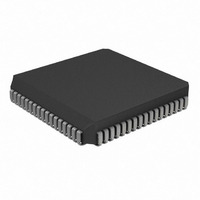
IC MCU OTP 16KX16 A/D 68PLCC
Manufacturer
Microchip Technology
Series
PIC® 17Cr
Specifications of PIC17LC756A-08/L
Core Processor
PIC
Core Size
8-Bit
Speed
8MHz
Connectivity
I²C, SPI, UART/USART
Peripherals
Brown-out Detect/Reset, POR, PWM, WDT
Number Of I /o
50
Program Memory Size
32KB (16K x 16)
Program Memory Type
OTP
Ram Size
902 x 8
Voltage - Supply (vcc/vdd)
3 V ~ 5.5 V
Data Converters
A/D 12x10b
Oscillator Type
External
Operating Temperature
0°C ~ 70°C
Package / Case
68-PLCC
Processor Series
PIC17LC
Core
PIC
Data Bus Width
8 bit
Data Ram Size
902 B
Interface Type
I2C, MSSP, RS- 232, SCI, SPI, USART
Maximum Clock Frequency
8 MHz
Number Of Programmable I/os
50
Number Of Timers
8
Operating Supply Voltage
3 V to 5.5 V
Maximum Operating Temperature
+ 70 C
Mounting Style
SMD/SMT
Minimum Operating Temperature
0 C
On-chip Adc
12 bit
Lead Free Status / RoHS Status
Lead free / RoHS Compliant
Eeprom Size
-
Lead Free Status / Rohs Status
Details
Available stocks
Company
Part Number
Manufacturer
Quantity
Price
Company:

Part Number:
PIC17LC756A-08/L
Manufacturer:
MICROCHIP
Quantity:
12 000
Company:
Part Number:
PIC17LC756A-08/L
Manufacturer:
Microchip Technology
Quantity:
10 000


PIC17C7XX
7.3
PIC17C7XX devices have a 16 x 16-bit hardware stack
(Figure 7-1). The stack is not part of either the program
or data memory space, and the stack pointer is neither
readable nor writable. The PC (Program Counter) is
“PUSH’d” onto the stack when a CALL or LCALL
instruction is executed, or an interrupt is acknowl-
edged. The stack is “POP’d” in the event of a RETURN,
RETLW, or a RETFIE instruction execution. PCLATH is
not affected by a “PUSH” or a “POP” operation.
The stack operates as a circular buffer, with the stack
pointer initialized to '0' after all RESETS. There is a
stack available bit (STKAV) to allow software to ensure
that the stack will not overflow. The STKAV bit is set
after a device RESET. When the stack pointer equals
Fh, STKAV is cleared. When the stack pointer rolls over
from Fh to 0h, the STKAV bit will be held clear until a
device RESET.
After the device is “PUSH’d” sixteen times (without a
“POP”), the seventeenth push overwrites the value
from the first push. The eighteenth push overwrites the
second push (and so on).
DS30289B-page 54
Note 1: There is not a status bit for stack under-
Stack Operation
2: There are no instruction mnemonics
3: After a RESET, if a “POP” operation
flow. The STKAV bit can be used to detect
the underflow which results in the stack
pointer being at the Top-of-Stack.
called PUSH or POP. These are actions
that occur from the execution of the CALL,
RETURN, RETLW and RETFIE instruc-
tions, or the vectoring to an interrupt
vector.
occurs before a “PUSH” operation, the
STKAV bit will be cleared. This will
appear as if the stack is full (underflow
has occurred). If a “PUSH” operation
occurs next (before another “POP”), the
STKAV bit will be locked clear. Only a
device RESET will cause this bit to set.
7.4
Indirect addressing is a mode of addressing data mem-
ory where the data memory address in the instruction
is not fixed. That is, the register that is to be read or
written can be modified by the program. This can be
useful for data tables in the data memory. Figure 7-6
shows the operation of indirect addressing. This
depicts the moving of the value to the data memory
address specified by the value of the FSR register.
Example 7-1 shows the use of indirect addressing to
clear RAM in a minimum number of instructions. A sim-
ilar concept could be used to move a defined number
of bytes (block) of data to the USART transmit register
(TXREG). The starting address of the block of data to
be transmitted could easily be modified by the program.
FIGURE 7-6:
7.4.1
The PIC17C7XX has four registers for indirect address-
ing. These registers are:
• INDF0 and FSR0
• INDF1 and FSR1
Registers INDF0 and INDF1 are not physically imple-
mented. Reading or writing to these registers activates
indirect addressing, with the value in the corresponding
FSR register being the address of the data. The FSR is
an 8-bit register and allows addressing anywhere in the
256-byte data memory address range. For banked
memory, the bank of memory accessed is specified by
the value in the BSR.
If file INDF0 (or INDF1) itself is read indirectly via an
FSR, all '0's are read (Zero bit is set). Similarly, if INDF0
(or INDF1) is written to indirectly, the operation will be
equivalent to a NOP, and the status bits are not affected.
Instruction
Executed
Instruction
Fetched
Indirect Addressing
Opcode
Opcode
INDIRECT ADDRESSING
REGISTERS
INDIRECT ADDRESSING
Address
8
2000 Microchip Technology Inc.
File
8
8
File = INDFx
FSR
RAM
Related parts for PIC17LC756A-08/L
Image
Part Number
Description
Manufacturer
Datasheet
Request
R

Part Number:
Description:
MICRO CTRL 16K LOW PWR 68PLCC
Manufacturer:
Microchip Technology
Datasheet:
Part Number:
Description:
MICRO CTRL 16K LOW PWR 64SDIP
Manufacturer:
Microchip Technology
Datasheet:
Part Number:
Description:
MICRO CTRL 16K LOW PWR 64SDIP
Manufacturer:
Microchip Technology
Datasheet:
Part Number:
Description:
MICRO CTRL 16K LOW PWR 68PLCC
Manufacturer:
Microchip Technology
Datasheet:

Part Number:
Description:
Manufacturer:
Microchip Technology Inc.
Datasheet:
Part Number:
Description:
Manufacturer:
Microchip Technology Inc.
Datasheet:
Part Number:
Description:
Manufacturer:
Microchip Technology Inc.
Datasheet:
Part Number:
Description:
Manufacturer:
Microchip Technology Inc.
Datasheet:
Part Number:
Description:
Manufacturer:
Microchip Technology Inc.
Datasheet:
Part Number:
Description:
Manufacturer:
Microchip Technology Inc.
Datasheet:
Part Number:
Description:
Manufacturer:
Microchip Technology Inc.
Datasheet: