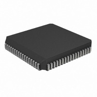
PIC17LC756A-08/L Microchip Technology, PIC17LC756A-08/L Datasheet - Page 72

PIC17LC756A-08/L
Manufacturer Part Number
PIC17LC756A-08/L
Description
IC MCU OTP 16KX16 A/D 68PLCC
Manufacturer
Microchip Technology
Series
PIC® 17Cr
Specifications of PIC17LC756A-08/L
Core Processor
PIC
Core Size
8-Bit
Speed
8MHz
Connectivity
I²C, SPI, UART/USART
Peripherals
Brown-out Detect/Reset, POR, PWM, WDT
Number Of I /o
50
Program Memory Size
32KB (16K x 16)
Program Memory Type
OTP
Ram Size
902 x 8
Voltage - Supply (vcc/vdd)
3 V ~ 5.5 V
Data Converters
A/D 12x10b
Oscillator Type
External
Operating Temperature
0°C ~ 70°C
Package / Case
68-PLCC
Processor Series
PIC17LC
Core
PIC
Data Bus Width
8 bit
Data Ram Size
902 B
Interface Type
I2C, MSSP, RS- 232, SCI, SPI, USART
Maximum Clock Frequency
8 MHz
Number Of Programmable I/os
50
Number Of Timers
8
Operating Supply Voltage
3 V to 5.5 V
Maximum Operating Temperature
+ 70 C
Mounting Style
SMD/SMT
Minimum Operating Temperature
0 C
On-chip Adc
12 bit
Lead Free Status / RoHS Status
Lead free / RoHS Compliant
Eeprom Size
-
Lead Free Status / Rohs Status
Details
Available stocks
Company
Part Number
Manufacturer
Quantity
Price
Company:
Part Number:
PIC17LC756A-08/L
Manufacturer:
MICROCHIP
Quantity:
12 000
Company:
Part Number:
PIC17LC756A-08/L
Manufacturer:
Microchip Technology
Quantity:
10 000
- Current page: 72 of 304
- Download datasheet (6Mb)
PIC17C7XX
10.1
PORTA is a 6-bit wide latch. PORTA does not have a
corresponding Data Direction Register (DDR). Upon a
device RESET, the PORTA pins are forced to be hi-
impedance inputs. For the RA4 and RA5 pins, the
peripheral module controls the output. When a device
RESET occurs, the peripheral module is disabled, so
these pins are forced to be hi-impedance inputs.
Reading PORTA reads the status of the pins.
The RA0 pin is multiplexed with the external interrupt,
INT. The RA1 pin is multiplexed with TMR0 clock input,
RA2 and RA3 are multiplexed with the SSP functions,
and RA4 and RA5 are multiplexed with the USART1
functions. The control of RA2, RA3, RA4 and RA5 as
outputs, is automatically configured by their multi-
plexed peripheral module when the module is enabled.
10.1.1
The RA2 and RA3 pins are open drain outputs. To use
the RA2 and/or the RA3 pin(s) as output(s), simply
write to the PORTA register the desired value. A ’0’ will
cause the pin to drive low, while a ’1’ will cause the pin
to float (hi-impedance). An external pull-up resistor
should be used to pull the pin high. Writes to the RA2
and RA3 pins will not affect the other PORTA pins.
DS30289B-page 72
Note:
PORTA Register
When using the RA2 or RA3 pin(s) as out-
put(s), read-modify-write instructions (such
as BCF, BSF, BTG) on PORTA are not
recommended.
Such operations read the port pins, do the
desired operation, and then write this value
to the data latch. This may inadvertently
cause the RA2 or RA3 pins to switch from
input to output (or vice-versa).
To avoid this possibility, use a shadow reg-
ister for PORTA. Do the bit operations on
this shadow register and then move it to
PORTA.
USING RA2, RA3 AS OUTPUTS
Example 10-1 shows an instruction sequence to initial-
ize PORTA. The Bank Select Register (BSR) must be
selected to Bank 0 for the port to be initialized. The fol-
lowing example uses the MOVLB instruction to load the
BSR register for bank selection.
EXAMPLE 10-1:
FIGURE 10-1:
FIGURE 10-2:
Note: Input pins have protection diodes to V
Note: I/O pin has protection diodes to V
MOVLB
MOVLW
MOVWF
0
0xF3
PORTA
1
0
D
; Select Bank 0
;
; Initialize PORTA
;
;
;
INITIALIZING PORTA
RA0 AND RA1 BLOCK
DIAGRAM
RA2 BLOCK DIAGRAM
Q
;
Q
EN
2000 Microchip Technology Inc.
RA<3:2> are output low
RA<5:4> and RA<1:0>
are inputs
(outputs floating)
Q
Peripheral Data In
CK
D
I
2
C Mode Enable
SS
SCL Out
WR_PORTA
RD_PORTA
DD
RD_PORTA
.
Data Bus
Data Bus
and V
(Q4)
(Q2)
(Q2)
SS
.
Related parts for PIC17LC756A-08/L
Image
Part Number
Description
Manufacturer
Datasheet
Request
R

Part Number:
Description:
MICRO CTRL 16K LOW PWR 68PLCC
Manufacturer:
Microchip Technology
Datasheet:

Part Number:
Description:
MICRO CTRL 16K LOW PWR 64SDIP
Manufacturer:
Microchip Technology
Datasheet:

Part Number:
Description:
MICRO CTRL 16K LOW PWR 64SDIP
Manufacturer:
Microchip Technology
Datasheet:

Part Number:
Description:
MICRO CTRL 16K LOW PWR 68PLCC
Manufacturer:
Microchip Technology
Datasheet:

Part Number:
Description:
Manufacturer:
Microchip Technology Inc.
Datasheet:

Part Number:
Description:
Manufacturer:
Microchip Technology Inc.
Datasheet:

Part Number:
Description:
Manufacturer:
Microchip Technology Inc.
Datasheet:

Part Number:
Description:
Manufacturer:
Microchip Technology Inc.
Datasheet:

Part Number:
Description:
Manufacturer:
Microchip Technology Inc.
Datasheet:

Part Number:
Description:
Manufacturer:
Microchip Technology Inc.
Datasheet:

Part Number:
Description:
Manufacturer:
Microchip Technology Inc.
Datasheet:


