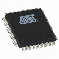
AT91SAM7X256B-AU Atmel, AT91SAM7X256B-AU Datasheet - Page 109

AT91SAM7X256B-AU
Manufacturer Part Number
AT91SAM7X256B-AU
Description
IC MCU 256KB FLASH 100LQFP
Manufacturer
Atmel
Series
AT91SAMr
Specifications of AT91SAM7X256B-AU
Core Processor
ARM7
Core Size
16/32-Bit
Speed
55MHz
Connectivity
CAN, Ethernet, I²C, SPI, SSC, UART/USART, USB
Peripherals
Brown-out Detect/Reset, DMA, POR, PWM, WDT
Number Of I /o
62
Program Memory Size
256KB (256K x 8)
Program Memory Type
FLASH
Ram Size
64K x 8
Voltage - Supply (vcc/vdd)
1.65 V ~ 1.95 V
Data Converters
A/D 8x10b
Oscillator Type
Internal
Operating Temperature
-40°C ~ 85°C
Package / Case
100-LQFP
Package
100LQFP
Device Core
ARM7TDMI
Family Name
91S
Maximum Speed
55 MHz
Operating Supply Voltage
1.8|3.3 V
Data Bus Width
32 Bit
Number Of Programmable I/os
62
Interface Type
CAN/Ethernet/SPI/I2S/TWI/USART/USB
On-chip Adc
8-chx10-bit
Number Of Timers
3
Controller Family/series
AT91SAM7xxxxx
No. Of I/o's
62
Ram Memory Size
64KB
Cpu Speed
55MHz
No. Of Timers
1
Rohs Compliant
Yes
Cpu Family
91S
Device Core Size
32b
Frequency (max)
55MHz
Total Internal Ram Size
64KB
# I/os (max)
62
Number Of Timers - General Purpose
3
Operating Supply Voltage (typ)
1.8/3.3V
Operating Supply Voltage (max)
1.95/3.6V
Operating Supply Voltage (min)
1.65/3V
Instruction Set Architecture
RISC
Operating Temp Range
-40C to 85C
Operating Temperature Classification
Industrial
Mounting
Surface Mount
Pin Count
100
Package Type
LQFP
Lead Free Status / RoHS Status
Lead free / RoHS Compliant
Eeprom Size
-
Lead Free Status / Rohs Status
Compliant
Available stocks
Company
Part Number
Manufacturer
Quantity
Price
Company:
Part Number:
AT91SAM7X256B-AU
Manufacturer:
Atmel
Quantity:
1 800
Part Number:
AT91SAM7X256B-AU
Manufacturer:
ATMEL/爱特梅尔
Quantity:
20 000
- Current page: 109 of 687
- Download datasheet (11Mb)
Figure 19-6. Example of Partial Page Programming:
19.2.4.2
6120H–ATARM–17-Feb-09
16 words
16 words
16 words
16 words
Erase All Command
FF
FF
FF
FF
FF
FF
FF
FF
FF
FF
FF
FF
Erase All Flash
Page 7 erased
32 bits wide
Step 1.
FF
FF
FF
FF
FF
FF
FF
FF
FF
FF
FF
FF
...
...
...
...
FF
FF
FF
FF
FF
FF
FF
FF
FF
FF
FF
FF
After programming, the page (the whole lock region) can be locked to prevent miscellaneous
write or erase sequences. The lock bit can be automatically set after page programming using
WPL.
Data to be written are stored in an internal latch buffer. The size of the latch buffer corresponds
to the page size. The latch buffer wraps around within the internal memory area address space
and appears to be repeated by the number of pages in it.
Note:
Data are written to the latch buffer before the programming command is written to the Flash
Command Register MC_FCR. The sequence is as follows:
Two errors can be detected in the MC_FSR register after a programming sequence:
The entire memory can be erased if the Erase All Command (EA) in the Flash Command Regis-
ter MC_FCR is written.
• Write the full page, at any page address, within the internal memory area address space
• Programming starts as soon as the page number and the programming command are written
• When programming is completed, the bit FRDY in the Flash Programming Status Register
• Programming Error: A bad keyword and/or an invalid command have been written in the
• Lock Error: The page to be programmed belongs to a locked region. A command must be
FF
FF
FF
FF
FF
FF
FF
FF
FF
FF
FF
FF
using only 32-bit access.
to the Flash Command Register. The FRDY bit in the Flash Programming Status Register
(MC_FSR) is automatically cleared.
(MC_FSR) rises. If an interrupt was enabled by setting the bit FRDY in MC_FMR, the
interrupt line of the Memory Controller is activated.
MC_FCR register.
previously run to unlock the corresponding region.
Writing of 8-bit and 16-bit data is not allowed and may lead to unpredictable data corruption.
Programming of the second part of Page 7
AT91SAM7X512/256/128 Preliminary
FF
FF
FF
CA FE
CA FE
CA FE
FF
FF
FF
FF
FF
FF
(NEBP = 1)
32 bits wide
FF
FF
FF
FF
FF
FF
FF
FF
FF
Step 2.
...
...
...
...
CA
CA
CA
FF
FF
FF
FF
FF
FF
FF
FF
FF
FF
FF
FF
FF
FF
FF
FF
FF
FF
FE
FE
FE
Programming of the third part of Page 7
CA FE
CA FE
CA FE
FF
FF
FF
DE CA
DE CA
DE CA
FF
FF
FF
(NEBP = 1)
32 bits wide
FF
FF
FF
FF
FF
FF
Step 3.
...
...
...
...
CA
CA
CA
FF
FF
FF
DE CA
DE CA
DE CA
FF
FF
FF
FF
FF
FF
FE
FE
FE
FF
FF
FF
109
Related parts for AT91SAM7X256B-AU
Image
Part Number
Description
Manufacturer
Datasheet
Request
R

Part Number:
Description:
KIT EVAL FOR AT91SAM7X256/128
Manufacturer:
Atmel
Datasheet:

Part Number:
Description:
MCU, MPU & DSP Development Tools KICKSTART KIT ATMEL AT91SAM7X
Manufacturer:
IAR Systems

Part Number:
Description:
MCU ARM9 64K SRAM 144-LFBGA
Manufacturer:
Atmel
Datasheet:

Part Number:
Description:
IC ARM7 MCU FLASH 256K 100LQFP
Manufacturer:
Atmel
Datasheet:

Part Number:
Description:
IC ARM9 MPU 217-LFBGA
Manufacturer:
Atmel
Datasheet:

Part Number:
Description:
MCU ARM9 ULTRA LOW PWR 217-LFBGA
Manufacturer:
Atmel
Datasheet:

Part Number:
Description:
MCU ARM9 324-TFBGA
Manufacturer:
Atmel
Datasheet:

Part Number:
Description:
IC MCU ARM9 SAMPLING 217CBGA
Manufacturer:
Atmel
Datasheet:

Part Number:
Description:
IC ARM9 MCU 217-LFBGA
Manufacturer:
Atmel
Datasheet:

Part Number:
Description:
IC ARM9 MCU 208-PQFP
Manufacturer:
Atmel
Datasheet:

Part Number:
Description:
MCU ARM 512K HS FLASH 100-LQFP
Manufacturer:
Atmel
Datasheet:

Part Number:
Description:
MCU ARM 512K HS FLASH 100-TFBGA
Manufacturer:
Atmel
Datasheet:

Part Number:
Description:
IC ARM9 MCU 200 MHZ 324-TFBGA
Manufacturer:
Atmel
Datasheet:

Part Number:
Description:
IC ARM MCU 16BIT 128K 256BGA
Manufacturer:
Atmel
Datasheet:

Part Number:
Description:
IC ARM7 MCU 32BIT 128K 64LQFP
Manufacturer:
Atmel
Datasheet:


