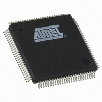
AT91SAM7X256B-AU Atmel, AT91SAM7X256B-AU Datasheet - Page 356

AT91SAM7X256B-AU
Manufacturer Part Number
AT91SAM7X256B-AU
Description
IC MCU 256KB FLASH 100LQFP
Manufacturer
Atmel
Series
AT91SAMr
Specifications of AT91SAM7X256B-AU
Core Processor
ARM7
Core Size
16/32-Bit
Speed
55MHz
Connectivity
CAN, Ethernet, I²C, SPI, SSC, UART/USART, USB
Peripherals
Brown-out Detect/Reset, DMA, POR, PWM, WDT
Number Of I /o
62
Program Memory Size
256KB (256K x 8)
Program Memory Type
FLASH
Ram Size
64K x 8
Voltage - Supply (vcc/vdd)
1.65 V ~ 1.95 V
Data Converters
A/D 8x10b
Oscillator Type
Internal
Operating Temperature
-40°C ~ 85°C
Package / Case
100-LQFP
Package
100LQFP
Device Core
ARM7TDMI
Family Name
91S
Maximum Speed
55 MHz
Operating Supply Voltage
1.8|3.3 V
Data Bus Width
32 Bit
Number Of Programmable I/os
62
Interface Type
CAN/Ethernet/SPI/I2S/TWI/USART/USB
On-chip Adc
8-chx10-bit
Number Of Timers
3
Controller Family/series
AT91SAM7xxxxx
No. Of I/o's
62
Ram Memory Size
64KB
Cpu Speed
55MHz
No. Of Timers
1
Rohs Compliant
Yes
Cpu Family
91S
Device Core Size
32b
Frequency (max)
55MHz
Total Internal Ram Size
64KB
# I/os (max)
62
Number Of Timers - General Purpose
3
Operating Supply Voltage (typ)
1.8/3.3V
Operating Supply Voltage (max)
1.95/3.6V
Operating Supply Voltage (min)
1.65/3V
Instruction Set Architecture
RISC
Operating Temp Range
-40C to 85C
Operating Temperature Classification
Industrial
Mounting
Surface Mount
Pin Count
100
Package Type
LQFP
Lead Free Status / RoHS Status
Lead free / RoHS Compliant
Eeprom Size
-
Lead Free Status / Rohs Status
Compliant
Available stocks
Company
Part Number
Manufacturer
Quantity
Price
Company:
Part Number:
AT91SAM7X256B-AU
Manufacturer:
Atmel
Quantity:
1 800
Part Number:
AT91SAM7X256B-AU
Manufacturer:
ATMEL/爱特梅尔
Quantity:
20 000
- Current page: 356 of 687
- Download datasheet (11Mb)
Figure 31-6. Transmitter Clock Management
31.6.1.3
Figure 31-7. Receiver Clock Management
31.6.1.4
356
AT91SAM7X512/256/128 Preliminary
Receiver Clock Management
Serial Clock Ratio Considerations
(CKS field) and at the same time Continuous Transmit Clock (CKO field) might lead to unpredict-
able results.
The receiver clock is generated from the transmitter clock or the divider clock or an external
clock scanned on the RK I/O pad. The Receive Clock is selected by the CKS field in
SSC_RCMR (Receive Clock Mode Register). Receive Clocks can be inverted independently by
the CKI bits in SSC_RCMR.
The receiver can also drive the RK I/O pad continuously or be limited to the actual data transfer.
The clock output is configured by the SSC_RCMR register. The Receive Clock Inversion (CKI)
bits have no effect on the clock outputs. Programming the RCMR register to select RK pin (CKS
field) and at the same time Continuous Receive Clock (CKO field) can lead to unpredictable
results.
The Transmitter and the Receiver can be programmed to operate with the clock signals provided
on either the TK or RK pins. This allows the SSC to support many slave-mode data transfers. In
this case, the maximum clock speed allowed on the RK pin is:
In addition, the maximum clock speed allowed on the TK pin is:
Transmitter Clock
Receiver Clock
– Master Clock divided by 2 if Receiver Frame Synchro is input
– Master Clock divided by 3 if Receiver Frame Synchro is output
– Master Clock divided by 6 if Transmit Frame Synchro is input
– Master Clock divided by 2 if Transmit Frame Synchro is output
Divider Clock
Divider Clock
RK
TK
SSC_RCMR.CKS
SSC_TCMR.CKS
0
1
0
1
SSC_RCMR.CKO
SSC_TCMR.CKO
SSC_RCMR.CKI
SSC_TCMR.CKI
Receiver Clock
Transmitter Clock
RK
TK
6120H–ATARM–17-Feb-09
Related parts for AT91SAM7X256B-AU
Image
Part Number
Description
Manufacturer
Datasheet
Request
R

Part Number:
Description:
KIT EVAL FOR AT91SAM7X256/128
Manufacturer:
Atmel
Datasheet:

Part Number:
Description:
MCU, MPU & DSP Development Tools KICKSTART KIT ATMEL AT91SAM7X
Manufacturer:
IAR Systems

Part Number:
Description:
MCU ARM9 64K SRAM 144-LFBGA
Manufacturer:
Atmel
Datasheet:

Part Number:
Description:
IC ARM7 MCU FLASH 256K 100LQFP
Manufacturer:
Atmel
Datasheet:

Part Number:
Description:
IC ARM9 MPU 217-LFBGA
Manufacturer:
Atmel
Datasheet:

Part Number:
Description:
MCU ARM9 ULTRA LOW PWR 217-LFBGA
Manufacturer:
Atmel
Datasheet:

Part Number:
Description:
MCU ARM9 324-TFBGA
Manufacturer:
Atmel
Datasheet:

Part Number:
Description:
IC MCU ARM9 SAMPLING 217CBGA
Manufacturer:
Atmel
Datasheet:

Part Number:
Description:
IC ARM9 MCU 217-LFBGA
Manufacturer:
Atmel
Datasheet:

Part Number:
Description:
IC ARM9 MCU 208-PQFP
Manufacturer:
Atmel
Datasheet:

Part Number:
Description:
MCU ARM 512K HS FLASH 100-LQFP
Manufacturer:
Atmel
Datasheet:

Part Number:
Description:
MCU ARM 512K HS FLASH 100-TFBGA
Manufacturer:
Atmel
Datasheet:

Part Number:
Description:
IC ARM9 MCU 200 MHZ 324-TFBGA
Manufacturer:
Atmel
Datasheet:

Part Number:
Description:
IC ARM MCU 16BIT 128K 256BGA
Manufacturer:
Atmel
Datasheet:

Part Number:
Description:
IC ARM7 MCU 32BIT 128K 64LQFP
Manufacturer:
Atmel
Datasheet:


