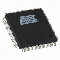
AT91SAM7X256B-AU Atmel, AT91SAM7X256B-AU Datasheet - Page 235

AT91SAM7X256B-AU
Manufacturer Part Number
AT91SAM7X256B-AU
Description
IC MCU 256KB FLASH 100LQFP
Manufacturer
Atmel
Series
AT91SAMr
Specifications of AT91SAM7X256B-AU
Core Processor
ARM7
Core Size
16/32-Bit
Speed
55MHz
Connectivity
CAN, Ethernet, I²C, SPI, SSC, UART/USART, USB
Peripherals
Brown-out Detect/Reset, DMA, POR, PWM, WDT
Number Of I /o
62
Program Memory Size
256KB (256K x 8)
Program Memory Type
FLASH
Ram Size
64K x 8
Voltage - Supply (vcc/vdd)
1.65 V ~ 1.95 V
Data Converters
A/D 8x10b
Oscillator Type
Internal
Operating Temperature
-40°C ~ 85°C
Package / Case
100-LQFP
Package
100LQFP
Device Core
ARM7TDMI
Family Name
91S
Maximum Speed
55 MHz
Operating Supply Voltage
1.8|3.3 V
Data Bus Width
32 Bit
Number Of Programmable I/os
62
Interface Type
CAN/Ethernet/SPI/I2S/TWI/USART/USB
On-chip Adc
8-chx10-bit
Number Of Timers
3
Controller Family/series
AT91SAM7xxxxx
No. Of I/o's
62
Ram Memory Size
64KB
Cpu Speed
55MHz
No. Of Timers
1
Rohs Compliant
Yes
Cpu Family
91S
Device Core Size
32b
Frequency (max)
55MHz
Total Internal Ram Size
64KB
# I/os (max)
62
Number Of Timers - General Purpose
3
Operating Supply Voltage (typ)
1.8/3.3V
Operating Supply Voltage (max)
1.95/3.6V
Operating Supply Voltage (min)
1.65/3V
Instruction Set Architecture
RISC
Operating Temp Range
-40C to 85C
Operating Temperature Classification
Industrial
Mounting
Surface Mount
Pin Count
100
Package Type
LQFP
Lead Free Status / RoHS Status
Lead free / RoHS Compliant
Eeprom Size
-
Lead Free Status / Rohs Status
Compliant
Available stocks
Company
Part Number
Manufacturer
Quantity
Price
Company:
Part Number:
AT91SAM7X256B-AU
Manufacturer:
Atmel
Quantity:
1 800
Part Number:
AT91SAM7X256B-AU
Manufacturer:
ATMEL/爱特梅尔
Quantity:
20 000
- Current page: 235 of 687
- Download datasheet (11Mb)
Figure 27-4. Output Line Timings
27.4.8
27.4.9
6120H–ATARM–17-Feb-09
Write PIO_ODSR at 1
Write PIO_ODSR at 0
Write PIO_CODR
Write PIO_SODR
Inputs
Input Glitch Filtering
PIO_ODSR
PIO_PDSR
MCK
The level on each I/O line can be read through PIO_PDSR (Pin Data Status Register). This reg-
ister indicates the level of the I/O lines regardless of their configuration, whether uniquely as an
input or driven by the PIO controller or driven by a peripheral.
Reading the I/O line levels requires the clock of the PIO controller to be enabled, otherwise
PIO_PDSR reads the levels present on the I/O line at the time the clock was disabled.
Optional input glitch filters are independently programmable on each I/O line. When the glitch fil-
ter is enabled, a glitch with a duration of less than 1/2 Master Clock (MCK) cycle is automatically
rejected, while a pulse with a duration of 1 Master Clock cycle or more is accepted. For pulse
durations between 1/2 Master Clock cycle and 1 Master Clock cycle the pulse may or may not
be taken into account, depending on the precise timing of its occurrence. Thus for a pulse to be
visible it must exceed 1 Master Clock cycle, whereas for a glitch to be reliably filtered out, its
duration must not exceed 1/2 Master Clock cycle. The filter introduces one Master Clock cycle
latency if the pin level change occurs before a rising edge. However, this latency does not
appear if the pin level change occurs before a falling edge. This is illustrated in
The glitch filters are controlled by the register set; PIO_IFER (Input Filter Enable Register),
PIO_IFDR (Input Filter Disable Register) and PIO_IFSR (Input Filter Status Register). Writing
PIO_IFER and PIO_IFDR respectively sets and clears bits in PIO_IFSR. This last register
enables the glitch filter on the I/O lines.
When the glitch filter is enabled, it does not modify the behavior of the inputs on the peripherals.
It acts only on the value read in PIO_PDSR and on the input change interrupt detection. The
glitch filters require that the PIO Controller clock is enabled.
APB Access
2 cycles
AT91SAM7X512/256/128 Preliminary
APB Access
2 cycles
Figure
27-5.
235
Related parts for AT91SAM7X256B-AU
Image
Part Number
Description
Manufacturer
Datasheet
Request
R

Part Number:
Description:
KIT EVAL FOR AT91SAM7X256/128
Manufacturer:
Atmel
Datasheet:

Part Number:
Description:
MCU, MPU & DSP Development Tools KICKSTART KIT ATMEL AT91SAM7X
Manufacturer:
IAR Systems

Part Number:
Description:
MCU ARM9 64K SRAM 144-LFBGA
Manufacturer:
Atmel
Datasheet:

Part Number:
Description:
IC ARM7 MCU FLASH 256K 100LQFP
Manufacturer:
Atmel
Datasheet:

Part Number:
Description:
IC ARM9 MPU 217-LFBGA
Manufacturer:
Atmel
Datasheet:

Part Number:
Description:
MCU ARM9 ULTRA LOW PWR 217-LFBGA
Manufacturer:
Atmel
Datasheet:

Part Number:
Description:
MCU ARM9 324-TFBGA
Manufacturer:
Atmel
Datasheet:

Part Number:
Description:
IC MCU ARM9 SAMPLING 217CBGA
Manufacturer:
Atmel
Datasheet:

Part Number:
Description:
IC ARM9 MCU 217-LFBGA
Manufacturer:
Atmel
Datasheet:

Part Number:
Description:
IC ARM9 MCU 208-PQFP
Manufacturer:
Atmel
Datasheet:

Part Number:
Description:
MCU ARM 512K HS FLASH 100-LQFP
Manufacturer:
Atmel
Datasheet:

Part Number:
Description:
MCU ARM 512K HS FLASH 100-TFBGA
Manufacturer:
Atmel
Datasheet:

Part Number:
Description:
IC ARM9 MCU 200 MHZ 324-TFBGA
Manufacturer:
Atmel
Datasheet:

Part Number:
Description:
IC ARM MCU 16BIT 128K 256BGA
Manufacturer:
Atmel
Datasheet:

Part Number:
Description:
IC ARM7 MCU 32BIT 128K 64LQFP
Manufacturer:
Atmel
Datasheet:


