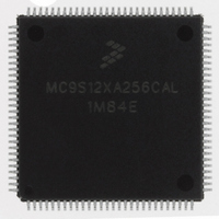
MC9S12XA256CAL Freescale Semiconductor, MC9S12XA256CAL Datasheet - Page 1007

MC9S12XA256CAL
Manufacturer Part Number
MC9S12XA256CAL
Description
IC MCU 256K FLASH 112-LQFP
Manufacturer
Freescale Semiconductor
Series
HCS12r
Specifications of MC9S12XA256CAL
Core Processor
HCS12X
Core Size
16-Bit
Speed
80MHz
Connectivity
EBI/EMI, I²C, IrDA, LIN, SCI, SPI
Peripherals
LVD, POR, PWM, WDT
Number Of I /o
91
Program Memory Size
256KB (256K x 8)
Program Memory Type
FLASH
Eeprom Size
4K x 8
Ram Size
16K x 8
Voltage - Supply (vcc/vdd)
2.35 V ~ 5.5 V
Data Converters
A/D 16x10b
Oscillator Type
External
Operating Temperature
-40°C ~ 85°C
Package / Case
112-LQFP
No. Of I/o's
91
Eeprom Memory Size
4KB
Ram Memory Size
16KB
Cpu Speed
80MHz
No. Of Timers
1
No. Of Pwm Channels
8
Digital Ic Case Style
LQFP
Rohs Compliant
Yes
Processor Series
S12XA
Core
HCS12
Data Bus Width
16 bit
Data Ram Size
16 KB
Interface Type
CAN, I2C, SCI, SPI
Maximum Clock Frequency
40 MHz
Number Of Programmable I/os
91
Number Of Timers
12
Maximum Operating Temperature
+ 85 C
Mounting Style
SMD/SMT
3rd Party Development Tools
EWHCS12
Development Tools By Supplier
EVB9S12XDP512E
Minimum Operating Temperature
- 40 C
On-chip Adc
2 (10 bit, 16 Channel)
Package
112LQFP
Family Name
HCS12
Maximum Speed
40 MHz
Operating Supply Voltage
2.5|5 V
Lead Free Status / RoHS Status
Lead free / RoHS Compliant
Available stocks
Company
Part Number
Manufacturer
Quantity
Price
Company:
Part Number:
MC9S12XA256CAL
Manufacturer:
AD
Quantity:
101
Company:
Part Number:
MC9S12XA256CAL
Manufacturer:
Freescale Semiconductor
Quantity:
10 000
Part Number:
MC9S12XA256CAL
Manufacturer:
FREESCALE
Quantity:
20 000
- Current page: 1007 of 1348
- Download datasheet (8Mb)
DDRM[7:0]
RDRM[7:0]
Reset
Reset
The DDRM bits revert to controlling the I/O direction of a pin when the associated peripheral
module is disabled.
Field
24.0.5.29 Port M Reduced Drive Register (RDRM)
Read: Anytime.
Write: Anytime.
This register configures the drive strength of each Port M output pin as either full or reduced. If the
port is used as input this bit is ignored.
Field
24.0.5.30 Port M Pull Device Enable Register (PERM)
Read: Anytime.
Write: Anytime.
7–0
7–0
W
W
R
R
RDRM7
PERM7
Data Direction Port M
0 Associated pin is configured as input.
1 Associated pin is configured as output.
Note: Due to internal synchronization circuits, it can take up to 2 bus clock cycles until the correct value is read
Reduced Drive Port M
0 Full drive strength at output.
1 Associated pin drives at about 1/6 of the full drive strength.
7
0
7
0
on PTM or PTIM registers, when changing the DDRM register.
RDRM6
PERM6
Figure 24-32. Port M Pull Device Enable Register (PERM)
0
0
6
6
Figure 24-31. Port M Reduced Drive Register (RDRM)
Table 24-29. DDRM Field Descriptions
Table 24-30. RDRM Field Descriptions
RDRM5
PERM5
5
0
5
0
RDRM4
PERM4
0
0
4
4
Description
Description
RDRM3
PERM3
3
0
3
0
RDRM2
PERM2
0
0
2
2
RDRM1
PERM1
1
0
1
0
RDRM0
PERM0
0
0
0
0
Related parts for MC9S12XA256CAL
Image
Part Number
Description
Manufacturer
Datasheet
Request
R
Part Number:
Description:
Manufacturer:
Freescale Semiconductor, Inc
Datasheet:
Part Number:
Description:
Manufacturer:
Freescale Semiconductor, Inc
Datasheet:
Part Number:
Description:
Manufacturer:
Freescale Semiconductor, Inc
Datasheet:
Part Number:
Description:
Manufacturer:
Freescale Semiconductor, Inc
Datasheet:
Part Number:
Description:
Manufacturer:
Freescale Semiconductor, Inc
Datasheet:
Part Number:
Description:
Manufacturer:
Freescale Semiconductor, Inc
Datasheet:
Part Number:
Description:
Manufacturer:
Freescale Semiconductor, Inc
Datasheet:
Part Number:
Description:
Manufacturer:
Freescale Semiconductor, Inc
Datasheet:
Part Number:
Description:
Manufacturer:
Freescale Semiconductor, Inc
Datasheet:
Part Number:
Description:
Manufacturer:
Freescale Semiconductor, Inc
Datasheet:
Part Number:
Description:
Manufacturer:
Freescale Semiconductor, Inc
Datasheet:
Part Number:
Description:
Manufacturer:
Freescale Semiconductor, Inc
Datasheet:
Part Number:
Description:
Manufacturer:
Freescale Semiconductor, Inc
Datasheet:
Part Number:
Description:
Manufacturer:
Freescale Semiconductor, Inc
Datasheet:
Part Number:
Description:
Manufacturer:
Freescale Semiconductor, Inc
Datasheet:


