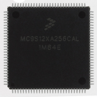
MC9S12XA256CAL Freescale Semiconductor, MC9S12XA256CAL Datasheet - Page 976

MC9S12XA256CAL
Manufacturer Part Number
MC9S12XA256CAL
Description
IC MCU 256K FLASH 112-LQFP
Manufacturer
Freescale Semiconductor
Series
HCS12r
Specifications of MC9S12XA256CAL
Core Processor
HCS12X
Core Size
16-Bit
Speed
80MHz
Connectivity
EBI/EMI, I²C, IrDA, LIN, SCI, SPI
Peripherals
LVD, POR, PWM, WDT
Number Of I /o
91
Program Memory Size
256KB (256K x 8)
Program Memory Type
FLASH
Eeprom Size
4K x 8
Ram Size
16K x 8
Voltage - Supply (vcc/vdd)
2.35 V ~ 5.5 V
Data Converters
A/D 16x10b
Oscillator Type
External
Operating Temperature
-40°C ~ 85°C
Package / Case
112-LQFP
No. Of I/o's
91
Eeprom Memory Size
4KB
Ram Memory Size
16KB
Cpu Speed
80MHz
No. Of Timers
1
No. Of Pwm Channels
8
Digital Ic Case Style
LQFP
Rohs Compliant
Yes
Processor Series
S12XA
Core
HCS12
Data Bus Width
16 bit
Data Ram Size
16 KB
Interface Type
CAN, I2C, SCI, SPI
Maximum Clock Frequency
40 MHz
Number Of Programmable I/os
91
Number Of Timers
12
Maximum Operating Temperature
+ 85 C
Mounting Style
SMD/SMT
3rd Party Development Tools
EWHCS12
Development Tools By Supplier
EVB9S12XDP512E
Minimum Operating Temperature
- 40 C
On-chip Adc
2 (10 bit, 16 Channel)
Package
112LQFP
Family Name
HCS12
Maximum Speed
40 MHz
Operating Supply Voltage
2.5|5 V
Lead Free Status / RoHS Status
Lead free / RoHS Compliant
Available stocks
Company
Part Number
Manufacturer
Quantity
Price
Company:
Part Number:
MC9S12XA256CAL
Manufacturer:
AD
Quantity:
101
Company:
Part Number:
MC9S12XA256CAL
Manufacturer:
Freescale Semiconductor
Quantity:
10 000
Part Number:
MC9S12XA256CAL
Manufacturer:
FREESCALE
Quantity:
20 000
- Current page: 976 of 1348
- Download datasheet (8Mb)
Chapter 24 DG128 Port Integration Module (S12XDG128PIMV2)
External Signal Description
This section lists and describes the signals that do connect off-chip.
24.0.3
Table 24-1
“Functional Description”
978
Port
—
A
B
E
K
T
Pin Name
PB[7:0]
PE[6:5]
PE[3:2]
PK[5:0]
PT[7:0]
PA[7:0]
BKGD
shows all the pins and their functions that are controlled by the PIM. Refer to
PE[7]
PE[4]
PE[1]
PE[0]
PK[7]
Signal Properties
If there is more than one function associated with a pin, the priority is
indicated by the position in the table from top (highest priority) to bottom
(lowest priority).
Pin Function
and Priority
XCLKS
ECLKX2
IOC[7:0]
MODC
BKGD
ECLK
GPIO
GPIO
GPIO
GPIO
GPIO
GPIO
GPIO
XIRQ
GPIO
GPIO
GPIO
GPIO
IRQ
Table 24-1. Pin Functions and Priorities (Sheet 1 of 5)
for the availability of the individual pins in the different package options.
1
1
MC9S12XDP512 Data Sheet, Rev. 2.21
I/O
I/O
I/O
I/O
I/O
I/O
I/O
I/O
I/O
I/O
I/O
I/O
I/O
I/O
O
I
I
I
I
I
MODC input during RESET
S12X_BDM communication pin
General-purpose I/O
General-purpose I/O
External clock selection input during RESET
Free-running clock output at Core Clock rate (ECLK x 2)
General-purpose I/O
General-purpose I/O
Free-running clock output at the Bus Clock rate or
programmable divided in normal modes
General-purpose I/O
General-purpose I/O
Maskable level- or falling edge-sensitive interrupt input
General-purpose I/O
Non-maskable level-sensitive interrupt input
General-purpose I/O
General-purpose I/O
General-purpose I/O
Enhanced Capture Timer Channels 7–0 input/output
General-purpose I/O
NOTE
Description
Freescale Semiconductor
Section ,
Pin Function
after Reset
BKGD
GPIO
GPIO
GPIO
GPIO
Related parts for MC9S12XA256CAL
Image
Part Number
Description
Manufacturer
Datasheet
Request
R
Part Number:
Description:
Manufacturer:
Freescale Semiconductor, Inc
Datasheet:
Part Number:
Description:
Manufacturer:
Freescale Semiconductor, Inc
Datasheet:
Part Number:
Description:
Manufacturer:
Freescale Semiconductor, Inc
Datasheet:
Part Number:
Description:
Manufacturer:
Freescale Semiconductor, Inc
Datasheet:
Part Number:
Description:
Manufacturer:
Freescale Semiconductor, Inc
Datasheet:
Part Number:
Description:
Manufacturer:
Freescale Semiconductor, Inc
Datasheet:
Part Number:
Description:
Manufacturer:
Freescale Semiconductor, Inc
Datasheet:
Part Number:
Description:
Manufacturer:
Freescale Semiconductor, Inc
Datasheet:
Part Number:
Description:
Manufacturer:
Freescale Semiconductor, Inc
Datasheet:
Part Number:
Description:
Manufacturer:
Freescale Semiconductor, Inc
Datasheet:
Part Number:
Description:
Manufacturer:
Freescale Semiconductor, Inc
Datasheet:
Part Number:
Description:
Manufacturer:
Freescale Semiconductor, Inc
Datasheet:
Part Number:
Description:
Manufacturer:
Freescale Semiconductor, Inc
Datasheet:
Part Number:
Description:
Manufacturer:
Freescale Semiconductor, Inc
Datasheet:
Part Number:
Description:
Manufacturer:
Freescale Semiconductor, Inc
Datasheet:


