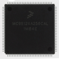
MC9S12XA256CAL Freescale Semiconductor, MC9S12XA256CAL Datasheet - Page 1226

MC9S12XA256CAL
Manufacturer Part Number
MC9S12XA256CAL
Description
IC MCU 256K FLASH 112-LQFP
Manufacturer
Freescale Semiconductor
Series
HCS12r
Specifications of MC9S12XA256CAL
Core Processor
HCS12X
Core Size
16-Bit
Speed
80MHz
Connectivity
EBI/EMI, I²C, IrDA, LIN, SCI, SPI
Peripherals
LVD, POR, PWM, WDT
Number Of I /o
91
Program Memory Size
256KB (256K x 8)
Program Memory Type
FLASH
Eeprom Size
4K x 8
Ram Size
16K x 8
Voltage - Supply (vcc/vdd)
2.35 V ~ 5.5 V
Data Converters
A/D 16x10b
Oscillator Type
External
Operating Temperature
-40°C ~ 85°C
Package / Case
112-LQFP
No. Of I/o's
91
Eeprom Memory Size
4KB
Ram Memory Size
16KB
Cpu Speed
80MHz
No. Of Timers
1
No. Of Pwm Channels
8
Digital Ic Case Style
LQFP
Rohs Compliant
Yes
Processor Series
S12XA
Core
HCS12
Data Bus Width
16 bit
Data Ram Size
16 KB
Interface Type
CAN, I2C, SCI, SPI
Maximum Clock Frequency
40 MHz
Number Of Programmable I/os
91
Number Of Timers
12
Maximum Operating Temperature
+ 85 C
Mounting Style
SMD/SMT
3rd Party Development Tools
EWHCS12
Development Tools By Supplier
EVB9S12XDP512E
Minimum Operating Temperature
- 40 C
On-chip Adc
2 (10 bit, 16 Channel)
Package
112LQFP
Family Name
HCS12
Maximum Speed
40 MHz
Operating Supply Voltage
2.5|5 V
Lead Free Status / RoHS Status
Lead free / RoHS Compliant
Available stocks
Company
Part Number
Manufacturer
Quantity
Price
Company:
Part Number:
MC9S12XA256CAL
Manufacturer:
AD
Quantity:
101
Company:
Part Number:
MC9S12XA256CAL
Manufacturer:
Freescale Semiconductor
Quantity:
10 000
Part Number:
MC9S12XA256CAL
Manufacturer:
FREESCALE
Quantity:
20 000
- Current page: 1226 of 1348
- Download datasheet (8Mb)
Chapter 29 128 Kbyte Flash Module (S12XFTX128K1V1)
between the written data and the backdoor key data stored in the Flash memory. If all four words of data
are written to the correct addresses in the correct order and the data matches the backdoor keys stored in
the Flash memory, the MCU will be unsecured. The data must be written to the backdoor keys sequentially
starting with 0x7F_FF00–1 and ending with 0x7F_FF06–7. 0x0000 and 0xFFFF are not permitted as
backdoor keys. While the KEYACC bit is set, reads of the Flash memory will return invalid data.
The user code stored in the Flash memory must have a method of receiving the backdoor keys from an
external stimulus. This external stimulus would typically be through one of the on-chip serial ports.
If the KEYEN[1:0] bits are in the enabled state (see
the MCU can be unsecured by the backdoor key access sequence described below:
The backdoor key access sequence is monitored by an internal security state machine. An illegal operation
during the backdoor key access sequence will cause the security state machine to lock, leaving the MCU
in the secured state. A reset of the MCU will cause the security state machine to exit the lock state and
allow a new backdoor key access sequence to be attempted. The following operations during the backdoor
key access sequence will lock the security state machine:
After the backdoor keys have been correctly matched, the MCU will be unsecured. Once the MCU is
unsecured, the Flash security byte can be programmed to the unsecure state, if desired.
In the unsecure state, the user has full control of the contents of the backdoor keys by programming
addresses 0x7F_FF00–0x7F_FF07 in the Flash Configuration Field.
The security as defined in the Flash security byte (0x7F_FF0F) is not changed by using the backdoor key
access sequence to unsecure. The backdoor keys stored in addresses 0x7F_FF00–0x7F_FF07 are
unaffected by the backdoor key access sequence. After the next reset of the MCU, the security state of the
Flash module is determined by the Flash security byte (0x7F_FF0F). The backdoor key access sequence
has no effect on the program and erase protections defined in the Flash protection register.
It is not possible to unsecure the MCU in special single chip mode by using the backdoor key access
sequence in background debug mode (BDM).
1228
1. Set the KEYACC bit in the Flash Configuration Register (FCNFG).
2. Write the correct four 16-bit words to Flash addresses 0xFF00–0xFF07 sequentially starting with
3. Clear the KEYACC bit. Depending on the user code used to write the backdoor keys, a wait cycle
4. If all four 16-bit words match the backdoor keys stored in Flash addresses
1. If any of the four 16-bit words does not match the backdoor keys programmed in the Flash array.
2. If the four 16-bit words are written in the wrong sequence.
3. If more than four 16-bit words are written.
4. If any of the four 16-bit words written are 0x0000 or 0xFFFF.
5. If the KEYACC bit does not remain set while the four 16-bit words are written.
6. If any two of the four 16-bit words are written on successive MCU clock cycles.
0x7F_FF00.
(NOP) may be required before clearing the KEYACC bit.
0x7F_FF00–0x7F_FF07, the MCU is unsecured and the SEC[1:0] bits in the FSEC register are
forced to the unsecure state of 1:0.
MC9S12XDP512 Data Sheet, Rev. 2.21
Section 29.3.2.2, “Flash Security Register
Freescale Semiconductor
(FSEC)”),
Related parts for MC9S12XA256CAL
Image
Part Number
Description
Manufacturer
Datasheet
Request
R
Part Number:
Description:
Manufacturer:
Freescale Semiconductor, Inc
Datasheet:
Part Number:
Description:
Manufacturer:
Freescale Semiconductor, Inc
Datasheet:
Part Number:
Description:
Manufacturer:
Freescale Semiconductor, Inc
Datasheet:
Part Number:
Description:
Manufacturer:
Freescale Semiconductor, Inc
Datasheet:
Part Number:
Description:
Manufacturer:
Freescale Semiconductor, Inc
Datasheet:
Part Number:
Description:
Manufacturer:
Freescale Semiconductor, Inc
Datasheet:
Part Number:
Description:
Manufacturer:
Freescale Semiconductor, Inc
Datasheet:
Part Number:
Description:
Manufacturer:
Freescale Semiconductor, Inc
Datasheet:
Part Number:
Description:
Manufacturer:
Freescale Semiconductor, Inc
Datasheet:
Part Number:
Description:
Manufacturer:
Freescale Semiconductor, Inc
Datasheet:
Part Number:
Description:
Manufacturer:
Freescale Semiconductor, Inc
Datasheet:
Part Number:
Description:
Manufacturer:
Freescale Semiconductor, Inc
Datasheet:
Part Number:
Description:
Manufacturer:
Freescale Semiconductor, Inc
Datasheet:
Part Number:
Description:
Manufacturer:
Freescale Semiconductor, Inc
Datasheet:
Part Number:
Description:
Manufacturer:
Freescale Semiconductor, Inc
Datasheet:


