MC9S12XA256CAL Freescale Semiconductor, MC9S12XA256CAL Datasheet - Page 558
MC9S12XA256CAL
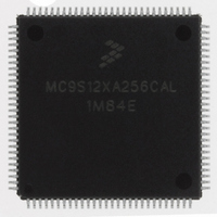
Manufacturer Part Number
MC9S12XA256CAL
Description
IC MCU 256K FLASH 112-LQFP
Manufacturer
Freescale Semiconductor
Series
HCS12r
Specifications of MC9S12XA256CAL
Core Processor
HCS12X
Core Size
16-Bit
Speed
80MHz
Connectivity
EBI/EMI, I²C, IrDA, LIN, SCI, SPI
Peripherals
LVD, POR, PWM, WDT
Number Of I /o
91
Program Memory Size
256KB (256K x 8)
Program Memory Type
FLASH
Eeprom Size
4K x 8
Ram Size
16K x 8
Voltage - Supply (vcc/vdd)
2.35 V ~ 5.5 V
Data Converters
A/D 16x10b
Oscillator Type
External
Operating Temperature
-40°C ~ 85°C
Package / Case
112-LQFP
No. Of I/o's
91
Eeprom Memory Size
4KB
Ram Memory Size
16KB
Cpu Speed
80MHz
No. Of Timers
1
No. Of Pwm Channels
8
Digital Ic Case Style
LQFP
Rohs Compliant
Yes
Processor Series
S12XA
Core
HCS12
Data Bus Width
16 bit
Data Ram Size
16 KB
Interface Type
CAN, I2C, SCI, SPI
Maximum Clock Frequency
40 MHz
Number Of Programmable I/os
91
Number Of Timers
12
Maximum Operating Temperature
+ 85 C
Mounting Style
SMD/SMT
3rd Party Development Tools
EWHCS12
Development Tools By Supplier
EVB9S12XDP512E
Minimum Operating Temperature
- 40 C
On-chip Adc
2 (10 bit, 16 Channel)
Package
112LQFP
Family Name
HCS12
Maximum Speed
40 MHz
Operating Supply Voltage
2.5|5 V
Lead Free Status / RoHS Status
Lead free / RoHS Compliant
Available stocks
Company
Part Number
Manufacturer
Quantity
Price
Company:

Part Number:
MC9S12XA256CAL
Manufacturer:
AD
Quantity:
101
Company:
Part Number:
MC9S12XA256CAL
Manufacturer:
Freescale Semiconductor
Quantity:
10 000
Part Number:
MC9S12XA256CAL
Manufacturer:
FREESCALE
Quantity:
20 000


Chapter 14 Voltage Regulator (S12VREG3V3V5)
14.2.4
Signals V
PLL and oscillator. These signals are connected to device pins to allow external decoupling capacitors
(220 nF, X7R ceramic).
In Shutdown Mode, an external supply driving V
14.2.5
This optional signal is used to shutdown VREG_3V3. In that case, V
provided externally. Shutdown mode is entered with VREGEN being low. If VREGEN is high, the
VREG_3V3 is either in Full Performance Mode or in Reduced Power Mode.
For the connectivity of VREGEN, see device specification.
14.3
This section provides a detailed description of all registers accessible in VREG_3V3.
If enabled in the system, the VREG_3V3 will abort all read and write accesses to reserved registers within
it’s memory slice.
14.3.1
Table 14-2
558
Address
0x0000
0x0001
0x0002
0x0003
0x0004
0x0005
0x0006
0x0007
DDPLL
Memory Map and Register Definition
Offset
provides an overview of all used registers.
VDDPLL, VSSPLL — Regulator Output2 (PLL) Pins
V
Module Memory Map
REGEN —
is not supported while MCU is powered.
Switching from FPM or RPM to shutdown of VREG_3V3 and vice versa
/V
SSPLL
are the secondary outputs of VREG_3V3 that provide the power supply for the
Autonomous Periodical Interrupt Trimming Register (VREGAPITR)
Optional Regulator Enable Pin
Autonomous Periodical Interrupt Control Register (VREGAPICL)
Autonomous Periodical Interrupt Period High (VREGAPIRH)
Autonomous Periodical Interrupt Period Low (VREGAPIRL)
MC9S12XDP512 Data Sheet, Rev. 2.21
HT Control Register (VREGHTCL)
Control Register (VREGCTRL)
Table 14-2. Memory Map
Reserved 06
Reserved 07
DDPLL
NOTE
Use
/V
SSPLL
can replace the voltage regulator.
DD
/V
SS
and V
DDPLL
Freescale Semiconductor
/V
Access
SSPLL
R/W
R/W
R/W
R/W
R/W
—
—
—
must be
Related parts for MC9S12XA256CAL
Image
Part Number
Description
Manufacturer
Datasheet
Request
R

Part Number:
Description:
Manufacturer:
Freescale Semiconductor, Inc
Datasheet:
Part Number:
Description:
Manufacturer:
Freescale Semiconductor, Inc
Datasheet:
Part Number:
Description:
Manufacturer:
Freescale Semiconductor, Inc
Datasheet:
Part Number:
Description:
Manufacturer:
Freescale Semiconductor, Inc
Datasheet:
Part Number:
Description:
Manufacturer:
Freescale Semiconductor, Inc
Datasheet:
Part Number:
Description:
Manufacturer:
Freescale Semiconductor, Inc
Datasheet:
Part Number:
Description:
Manufacturer:
Freescale Semiconductor, Inc
Datasheet:
Part Number:
Description:
Manufacturer:
Freescale Semiconductor, Inc
Datasheet:
Part Number:
Description:
Manufacturer:
Freescale Semiconductor, Inc
Datasheet:
Part Number:
Description:
Manufacturer:
Freescale Semiconductor, Inc
Datasheet:
Part Number:
Description:
Manufacturer:
Freescale Semiconductor, Inc
Datasheet:
Part Number:
Description:
Manufacturer:
Freescale Semiconductor, Inc
Datasheet:
Part Number:
Description:
Manufacturer:
Freescale Semiconductor, Inc
Datasheet:
Part Number:
Description:
Manufacturer:
Freescale Semiconductor, Inc
Datasheet:
Part Number:
Description:
Manufacturer:
Freescale Semiconductor, Inc
Datasheet: