M30280FCHP#U5B Renesas Electronics America, M30280FCHP#U5B Datasheet - Page 289
M30280FCHP#U5B
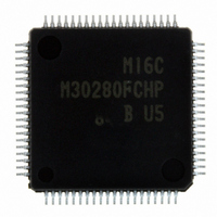
Manufacturer Part Number
M30280FCHP#U5B
Description
IC M16C/28 MCU FLASH 128K 80LQFP
Manufacturer
Renesas Electronics America
Series
M16C™ M16C/Tiny/28r
Datasheet
1.M30280F6HPU9.pdf
(425 pages)
Specifications of M30280FCHP#U5B
Core Processor
M16C/60
Core Size
16-Bit
Speed
20MHz
Connectivity
I²C, IEBus, SIO, UART/USART
Peripherals
DMA, POR, PWM, Voltage Detect, WDT
Number Of I /o
71
Program Memory Size
128KB (128K x 8)
Program Memory Type
FLASH
Ram Size
12K x 8
Voltage - Supply (vcc/vdd)
2.7 V ~ 5.5 V
Data Converters
A/D 24x10b
Oscillator Type
Internal
Operating Temperature
-20°C ~ 85°C
Package / Case
80-LQFP
For Use With
R0K330290S000BE - KIT EVAL STARTER FOR M16C/29M30290T2-CPE - EMULATOR COMPACT M16C/26A/28/29M30290T2-CPE-HP - EMULATOR COMPACT FOR M16C/TINY
Lead Free Status / RoHS Status
Lead free / RoHS Compliant
Eeprom Size
-
Available stocks
Company
Part Number
Manufacturer
Quantity
Price

Part Number:
M30280FCHP#U5BM30280FCHP#U3B
Manufacturer:
Renesas Electronics America
Quantity:
10 000
Part Number:
M30280FCHP#U5BM30280FCHP#U7B
Manufacturer:
Renesas Electronics America
Quantity:
10 000


R
R
M
16.6 I
e
E
1
. v
J
6
Table16.4 Timing of Interrupt Generation in Data Receive Mode
1) Synchronized with the falling edge of the
2) Synchronized with the falling edge of the
0
C
The S3D0 register controls the I
16.6.1 Bit 0 : Interrupt Enable Bit by STOP Condition (SIM )
16.6.2 Bit 1: Interrupt Enable Bit at the Completion of Data Receive (WIT)
I
2
9
2
ACK clock
The internal WAIT flag can be read by reading the WIT bit. The internal WAIT flag is set to "1" after writing
data to the S00 register and it is set to "0" after writing to the S20 register.
Consequently, the I
(See Figure 16.12)
When the data is transmitted and the address data is received immediately after the START condition,
the WAIT flag remains "0" regardless of the WIT bit setting, and the I
only generated at the falling edge of the ACK clock. Set the WIT bit to “0” when the ACK-CLK bit in the
S20 register is set to "0" (no ACK clock).
0 .
2 /
B
The SIM bit enables the I
is set to “1”, the I
change in the PIN flag).
When the WIT bit is set to "1" (enable the I2C bus interface interrupt upon completion of receiving data)
while the ACK-CLK bit in the S20 register is set to "1" (ACK clock), the I
is generated, synchronizing with the falling edge of the last data bit clock, and the PIN bit is set to "0"
(request interrupt) . Then an "L" signal is applied to the SCL
trolled. Table 16.4 and Figure 16.12 show the interrupt generation timing and the procedure of commu-
nication restart. After the communication is restarted, the PIN bit is set to "0" again, synchronized with the
falling edge of the ACK clock, and the I
C bus Interface Interrupt Generation Timing
last data bit clock
0
0
8
0
4
G
2
J
7
a
C0 Control Register 1 (S3D0 register)
o r
0 -
. n
u
2
3
p
0
, 1
0
(
M
2
0
1
0
6
7
C
2
2 /
C bus interface interrupt request is generated by the STOP condition detect (no need to
page 267
2
, 8
C bus interface interrupt request generated by the timing 1) or 2) can be determined.
M
1
6
2
C bus interface interrupt request by detecting a STOP condition. If the SIM bit
C
f o
2 /
8
2
3
) B
C bus interface circuit.
8
5
2
C bus interface interrupt request is generated.
Set the ACK bit in the S20 register.
Set the PIN bit to "1".
Set the S00 register
(Do not write to the S00 register. The ACK clock
operation may be unstable.)
Procedure of Communication Restart
MM
16. MULTI-MASTER I
and the ACK clock generation is con-
2
C bus interface interrupt request is
2
C bus interface interrupt request
2
C bus INTERFACE
Related parts for M30280FCHP#U5B
Image
Part Number
Description
Manufacturer
Datasheet
Request
R

Part Number:
Description:
KIT STARTER FOR M16C/29
Manufacturer:
Renesas Electronics America
Datasheet:

Part Number:
Description:
KIT STARTER FOR R8C/2D
Manufacturer:
Renesas Electronics America
Datasheet:

Part Number:
Description:
R0K33062P STARTER KIT
Manufacturer:
Renesas Electronics America
Datasheet:

Part Number:
Description:
KIT STARTER FOR R8C/23 E8A
Manufacturer:
Renesas Electronics America
Datasheet:

Part Number:
Description:
KIT STARTER FOR R8C/25
Manufacturer:
Renesas Electronics America
Datasheet:

Part Number:
Description:
KIT STARTER H8S2456 SHARPE DSPLY
Manufacturer:
Renesas Electronics America
Datasheet:

Part Number:
Description:
KIT STARTER FOR R8C38C
Manufacturer:
Renesas Electronics America
Datasheet:

Part Number:
Description:
KIT STARTER FOR R8C35C
Manufacturer:
Renesas Electronics America
Datasheet:

Part Number:
Description:
KIT STARTER FOR R8CL3AC+LCD APPS
Manufacturer:
Renesas Electronics America
Datasheet:
Part Number:
Description:
KIT STARTER FOR RX610
Manufacturer:
Renesas Electronics America
Datasheet:

Part Number:
Description:
KIT STARTER FOR R32C/118
Manufacturer:
Renesas Electronics America
Datasheet:

Part Number:
Description:
KIT DEV RSK-R8C/26-29
Manufacturer:
Renesas Electronics America
Datasheet:

Part Number:
Description:
KIT STARTER FOR SH7124
Manufacturer:
Renesas Electronics America
Datasheet:

Part Number:
Description:
KIT STARTER FOR H8SX/1622
Manufacturer:
Renesas Electronics America
Datasheet:

Part Number:
Description:
KIT DEV FOR SH7203
Manufacturer:
Renesas Electronics America
Datasheet: