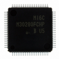
M30280FCHP#U5B Renesas Electronics America, M30280FCHP#U5B Datasheet - Page 303

M30280FCHP#U5B
Manufacturer Part Number
M30280FCHP#U5B
Description
IC M16C/28 MCU FLASH 128K 80LQFP
Manufacturer
Renesas Electronics America
Series
M16C™ M16C/Tiny/28r
Datasheet
1.M30280F6HPU9.pdf
(425 pages)
Specifications of M30280FCHP#U5B
Core Processor
M16C/60
Core Size
16-Bit
Speed
20MHz
Connectivity
I²C, IEBus, SIO, UART/USART
Peripherals
DMA, POR, PWM, Voltage Detect, WDT
Number Of I /o
71
Program Memory Size
128KB (128K x 8)
Program Memory Type
FLASH
Ram Size
12K x 8
Voltage - Supply (vcc/vdd)
2.7 V ~ 5.5 V
Data Converters
A/D 24x10b
Oscillator Type
Internal
Operating Temperature
-20°C ~ 85°C
Package / Case
80-LQFP
For Use With
R0K330290S000BE - KIT EVAL STARTER FOR M16C/29M30290T2-CPE - EMULATOR COMPACT M16C/26A/28/29M30290T2-CPE-HP - EMULATOR COMPACT FOR M16C/TINY
Lead Free Status / RoHS Status
Lead free / RoHS Compliant
Eeprom Size
-
Available stocks
Company
Part Number
Manufacturer
Quantity
Price
Part Number:
M30280FCHP#U5BM30280FCHP#U3B
Manufacturer:
Renesas Electronics America
Quantity:
10 000
Part Number:
M30280FCHP#U5BM30280FCHP#U7B
Manufacturer:
Renesas Electronics America
Quantity:
10 000
- Current page: 303 of 425
- Download datasheet (4Mb)
R
R
M
e
E
1
. v
J
6
Figure 16.24 The time of generation of RESTART condition
0
(2) Generation of RESTART condition
C
2
9
(3) Iimitation of CPU clock
0 .
2 /
B
S
S
S1I writing signal
( START condition setting standby)
S0I writing signal
(START condition trigger generation)
enter START condition standby mode and leave the SDA
by setting the S00 register after inserting a sufficient software wait until the SDA
("H") signal. Figure 16.24 shows the RESTART condition generation timing.
0
0
In order to generate a RESTART condition after 1-byte data transfer, write “E0
8
CL
DA
0
When the CM07 bit in the CM0 register is set to "1" (subclock), each register of the I
circuit cannot be read or written. Read or write data when the CM07 bit is set to "0" (main clock, PLL
clock, or on-chip oscillator clock).
4
G
J
7
a
o r
0 -
. n
u
2
3
p
0
, 1
0
(
8 clock
M
2
0
1
0
6
7
C
2 /
page 281
, 8
M
1
6
C
f o
2 /
8
3
) B
8
5
ACK
clock
MM
Insert software wait
open. Generate a START condition trigger
16. MULTI-MASTER I
MM
16
” to the S10 register,
outputs a high-level
2
2
C bus INTERFACE
C bus interface
Related parts for M30280FCHP#U5B
Image
Part Number
Description
Manufacturer
Datasheet
Request
R

Part Number:
Description:
KIT STARTER FOR M16C/29
Manufacturer:
Renesas Electronics America
Datasheet:

Part Number:
Description:
KIT STARTER FOR R8C/2D
Manufacturer:
Renesas Electronics America
Datasheet:

Part Number:
Description:
R0K33062P STARTER KIT
Manufacturer:
Renesas Electronics America
Datasheet:

Part Number:
Description:
KIT STARTER FOR R8C/23 E8A
Manufacturer:
Renesas Electronics America
Datasheet:

Part Number:
Description:
KIT STARTER FOR R8C/25
Manufacturer:
Renesas Electronics America
Datasheet:

Part Number:
Description:
KIT STARTER H8S2456 SHARPE DSPLY
Manufacturer:
Renesas Electronics America
Datasheet:

Part Number:
Description:
KIT STARTER FOR R8C38C
Manufacturer:
Renesas Electronics America
Datasheet:

Part Number:
Description:
KIT STARTER FOR R8C35C
Manufacturer:
Renesas Electronics America
Datasheet:

Part Number:
Description:
KIT STARTER FOR R8CL3AC+LCD APPS
Manufacturer:
Renesas Electronics America
Datasheet:

Part Number:
Description:
KIT STARTER FOR RX610
Manufacturer:
Renesas Electronics America
Datasheet:

Part Number:
Description:
KIT STARTER FOR R32C/118
Manufacturer:
Renesas Electronics America
Datasheet:

Part Number:
Description:
KIT DEV RSK-R8C/26-29
Manufacturer:
Renesas Electronics America
Datasheet:

Part Number:
Description:
KIT STARTER FOR SH7124
Manufacturer:
Renesas Electronics America
Datasheet:

Part Number:
Description:
KIT STARTER FOR H8SX/1622
Manufacturer:
Renesas Electronics America
Datasheet:

Part Number:
Description:
KIT DEV FOR SH7203
Manufacturer:
Renesas Electronics America
Datasheet:


