M30835FJGP#U5 Renesas Electronics America, M30835FJGP#U5 Datasheet - Page 109
M30835FJGP#U5
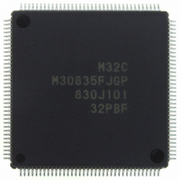
Manufacturer Part Number
M30835FJGP#U5
Description
IC M32C/83 MCU FLASH 144LQFP
Manufacturer
Renesas Electronics America
Series
M16C™ M32C/80r
Datasheets
1.M3087BFLGPU3.pdf
(364 pages)
2.M30833FJGPU3.pdf
(96 pages)
3.M30833FJGPU3.pdf
(529 pages)
Specifications of M30835FJGP#U5
Core Processor
M32C/80
Core Size
16/32-Bit
Speed
32MHz
Connectivity
CAN, I²C, IEBus, SIO, UART/USART
Peripherals
DMA, WDT
Number Of I /o
121
Program Memory Size
512KB (512K x 8)
Program Memory Type
FLASH
Ram Size
31K x 8
Voltage - Supply (vcc/vdd)
3 V ~ 5.5 V
Data Converters
A/D 34x10b, D/A 2x8b
Oscillator Type
Internal
Operating Temperature
-20°C ~ 85°C
Package / Case
144-LQFP
For Use With
R0K330879S001BE - KIT DEV RSK M32C/87R0K330879S000BE - KIT DEV RSK M32C/87
Lead Free Status / RoHS Status
Lead free / RoHS Compliant
Eeprom Size
-
Available stocks
Company
Part Number
Manufacturer
Quantity
Price

Part Number:
M30835FJGP#U5M30835FJGP#U3
Manufacturer:
Renesas Electronics America
Quantity:
10 000


R
R
M
e
E
3
. v
J
Table 8.7 Interrupts to Exit Wait Mode
2
0
8.5.3 Stop Mode
1
C
9
_______
NMI Interrupt
Serial I/O Interrupt
Key Input Interrupt
A/D Conversion Interrupt Available in single or single-sweep mode Do not use
Timer A Interrupt
Timer B Interrupt
______
INT Interrupt
CAN Interrupt
Intelligent I/O Interrupt
3 .
B
8 /
In stop mode, all oscillators and resonators stop. The CPU clock and peripheral function clock, as well as
the CPU and peripheral functions operated by these clocks, also stop. The least power required to
operate the microcomputer is in stop mode. The internal RAM holds its data if the voltage applied to the
Vcc pin is 2.5V or more.
Interrupts used to exit stop mode are NMI interrupt, key input interrupt, and INT interrupt.
0
1
8.5.3.1 Entering Stop Mode
3
0
Stop mode is entered when setting the CM10 bit in the CM1 register to "1" (all clocks stops). The
MCD4 to MCD0 bits in the MCD register become set to "01000
Enter stop mode after setting the followings.
3
J
G
4
• Initial Setting
• Before Entering Stop Mode
a
0 -
o r
n
Set each interrupt priority level after setting the minimum interrupt priority level required to exit stop
or wait mode, controlled by the RLVL2 to RLVL0 bits in the RLVL register, to "7".
(1) Set the I flag to "0"
(2) Set the interrupt priority level of the interrupt being used to exit stop mode
(3) Set the interrupt priority levels of the interrupts, not being used to exit stop mode, to "0"
(4) Set IPL in the FLG register. Then set the exit priority level to the same level as IPL
(5) Set the PRC0 bit in the PRCR register to "1" (write enabled)
(6) Select the main clock as the CPU clock
Interrupt
• When the CPU clock source is the sub clock,
• When the CPU clock source is the PLL clock,
• When the CPU clock source is the on-chip oscillator clock,
3 .
1
u
Set the CM05 bit in the CM0 register to "0" (main clock oscillates) and CM07 bit in the CM0
register to "0" (clock selected by the CM21 bit divided by MCD register setting)
Set the CM17 bit in the CM1 register to "0" (main clock) and the PLC07 bit in the PLC0 register to
"0" (PLL off)
Set the MCD4 to MCD0 bits to "01000
oscillates), and the CM21 it in the CM2 register to "0" (clock selected by the CM17 bit)
3
, 1
(Interrupt priority level of the interrupt used to exit stop mode > interrupt priority level to exit stop
p
mode
1
(
2
M
0
0
3
6
2
C
interrupt priority level of the interrupts not used to exit stop mode)
8 /
Page 84
, 3
Available
Available when the internal and external
clocks are used
Available
Available in all modes
Available
Available
Available
M
3
2
C
f o
8 /
4
3
8
) T
8
When CM02=0
______
2
" (divide-by-8 mode), the CM05 bit to "0" (main clock
Available
Available only when the external clock is used
Available
Available in event counter mode or when
the count source is f
Available
Do not use
Do not use
2
" (divide-by-8 mode).
______
When CM02=1
8. Clock Generation Circuit
C32
Related parts for M30835FJGP#U5
Image
Part Number
Description
Manufacturer
Datasheet
Request
R

Part Number:
Description:
KIT STARTER FOR M16C/29
Manufacturer:
Renesas Electronics America
Datasheet:

Part Number:
Description:
KIT STARTER FOR R8C/2D
Manufacturer:
Renesas Electronics America
Datasheet:

Part Number:
Description:
R0K33062P STARTER KIT
Manufacturer:
Renesas Electronics America
Datasheet:

Part Number:
Description:
KIT STARTER FOR R8C/23 E8A
Manufacturer:
Renesas Electronics America
Datasheet:

Part Number:
Description:
KIT STARTER FOR R8C/25
Manufacturer:
Renesas Electronics America
Datasheet:

Part Number:
Description:
KIT STARTER H8S2456 SHARPE DSPLY
Manufacturer:
Renesas Electronics America
Datasheet:

Part Number:
Description:
KIT STARTER FOR R8C38C
Manufacturer:
Renesas Electronics America
Datasheet:

Part Number:
Description:
KIT STARTER FOR R8C35C
Manufacturer:
Renesas Electronics America
Datasheet:

Part Number:
Description:
KIT STARTER FOR R8CL3AC+LCD APPS
Manufacturer:
Renesas Electronics America
Datasheet:
Part Number:
Description:
KIT STARTER FOR RX610
Manufacturer:
Renesas Electronics America
Datasheet:

Part Number:
Description:
KIT STARTER FOR R32C/118
Manufacturer:
Renesas Electronics America
Datasheet:

Part Number:
Description:
KIT DEV RSK-R8C/26-29
Manufacturer:
Renesas Electronics America
Datasheet:

Part Number:
Description:
KIT STARTER FOR SH7124
Manufacturer:
Renesas Electronics America
Datasheet:

Part Number:
Description:
KIT STARTER FOR H8SX/1622
Manufacturer:
Renesas Electronics America
Datasheet:

Part Number:
Description:
KIT DEV FOR SH7203
Manufacturer:
Renesas Electronics America
Datasheet: