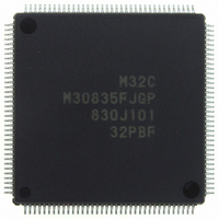
M30835FJGP#U5 Renesas Electronics America, M30835FJGP#U5 Datasheet - Page 419

M30835FJGP#U5
Manufacturer Part Number
M30835FJGP#U5
Description
IC M32C/83 MCU FLASH 144LQFP
Manufacturer
Renesas Electronics America
Series
M16C™ M32C/80r
Datasheets
1.M3087BFLGPU3.pdf
(364 pages)
2.M30833FJGPU3.pdf
(96 pages)
3.M30833FJGPU3.pdf
(529 pages)
Specifications of M30835FJGP#U5
Core Processor
M32C/80
Core Size
16/32-Bit
Speed
32MHz
Connectivity
CAN, I²C, IEBus, SIO, UART/USART
Peripherals
DMA, WDT
Number Of I /o
121
Program Memory Size
512KB (512K x 8)
Program Memory Type
FLASH
Ram Size
31K x 8
Voltage - Supply (vcc/vdd)
3 V ~ 5.5 V
Data Converters
A/D 34x10b, D/A 2x8b
Oscillator Type
Internal
Operating Temperature
-20°C ~ 85°C
Package / Case
144-LQFP
For Use With
R0K330879S001BE - KIT DEV RSK M32C/87R0K330879S000BE - KIT DEV RSK M32C/87
Lead Free Status / RoHS Status
Lead free / RoHS Compliant
Eeprom Size
-
Available stocks
Company
Part Number
Manufacturer
Quantity
Price
Part Number:
M30835FJGP#U5M30835FJGP#U3
Manufacturer:
Renesas Electronics America
Quantity:
10 000
- Current page: 419 of 529
- Download datasheet (5Mb)
R
R
M
25.3 CPU Rewrite Mode
e
E
3
. v
J
Table 25.3 Software Commands
2
SRD:
WA:
WD:
BA:
D
X:
xx:
0
Clear Status Register
In CPU rewrite mode, the user ROM area can be rewritten when the CPU executes software commands.
The user ROM area can be rewritten with the microcomputer mounted on a board, without using a parallel
or serial programmer.
Write the rewrite control program to either the user ROM area or the boot ROM area, beforehand. No
program in the flash memory can be executed in CPU rewrite mode. Therefore, transfer rewrite control
program to an area other than flash memory (internal RAM, etc.), and execute.
CPU rewrite mode can be entered when the microcomputer is in single-chip, memory expansion, and boot
mode.
Software commands, listed in Table 25.3, can be used in CPU rewrite mode. Refer to 25.3.3 Software
Command for details of each command.
Read or write commands and data from or to even addresses in the user ROM area, in 16-bit units. The 8
high-order bits (D
Read Array
Read Status Register
Page Program
Block Erase
Erase All Unlocked Block
Read Lock Bit Status
Lock Bit Program
1
9
C
6
:
3 .
B
8 /
Software Command
0
1
3
0
3
J
Data in the SRD register (D
Address to be written (Increment A
16-bit write data
Highest-order block address (A
Lock bit (D
Any even address in the user ROM area (A
8 high-order bits of command code (ignored)
G
4
a
0 -
n
o r
3 .
1
u
, 1
3
p
1
2
(
M
0
6
0
=1: unlock, D
3
6
2
15
C
8 /
Page 394
to D
, 3
M
8
Mode
Write
Write
Write
Write
Write
Write
Write
Write
) are ignored when writing command codes.
6
3
=0: locked)
2
7
C
f o
to D
8 /
First Bus Cycle
0
4
= 0)
3
Address
0
8
)
) T
8
7
to A
X
X
X
X
X
X
X
X
0
by 2 from "00
0
(D
= 0)
xxFF
xxA7
xx70
xx50
xx41
xx20
xx77
xx71
15
Data
to D
16
16
16
16
16
16
16
16
0
)
16
" to "FE
Mode
Read
Write
Write
Write
Write
Read
Second Bus Cycle
16
Address
".)
WA
BA
BA
BA
X
X
(D
xxD0
xxD0
xxD0
15
Data
SRD
WD
D
to D
6
16
16
16
0
)
Mode
Write
25. Flash Memory Version
Third Bus Cycle
Address
WA+2
(D
15
Data
WD
to D
0
)
Related parts for M30835FJGP#U5
Image
Part Number
Description
Manufacturer
Datasheet
Request
R

Part Number:
Description:
KIT STARTER FOR M16C/29
Manufacturer:
Renesas Electronics America
Datasheet:

Part Number:
Description:
KIT STARTER FOR R8C/2D
Manufacturer:
Renesas Electronics America
Datasheet:

Part Number:
Description:
R0K33062P STARTER KIT
Manufacturer:
Renesas Electronics America
Datasheet:

Part Number:
Description:
KIT STARTER FOR R8C/23 E8A
Manufacturer:
Renesas Electronics America
Datasheet:

Part Number:
Description:
KIT STARTER FOR R8C/25
Manufacturer:
Renesas Electronics America
Datasheet:

Part Number:
Description:
KIT STARTER H8S2456 SHARPE DSPLY
Manufacturer:
Renesas Electronics America
Datasheet:

Part Number:
Description:
KIT STARTER FOR R8C38C
Manufacturer:
Renesas Electronics America
Datasheet:

Part Number:
Description:
KIT STARTER FOR R8C35C
Manufacturer:
Renesas Electronics America
Datasheet:

Part Number:
Description:
KIT STARTER FOR R8CL3AC+LCD APPS
Manufacturer:
Renesas Electronics America
Datasheet:

Part Number:
Description:
KIT STARTER FOR RX610
Manufacturer:
Renesas Electronics America
Datasheet:

Part Number:
Description:
KIT STARTER FOR R32C/118
Manufacturer:
Renesas Electronics America
Datasheet:

Part Number:
Description:
KIT DEV RSK-R8C/26-29
Manufacturer:
Renesas Electronics America
Datasheet:

Part Number:
Description:
KIT STARTER FOR SH7124
Manufacturer:
Renesas Electronics America
Datasheet:

Part Number:
Description:
KIT STARTER FOR H8SX/1622
Manufacturer:
Renesas Electronics America
Datasheet:

Part Number:
Description:
KIT DEV FOR SH7203
Manufacturer:
Renesas Electronics America
Datasheet:


