M30835FJGP#U5 Renesas Electronics America, M30835FJGP#U5 Datasheet - Page 424
M30835FJGP#U5
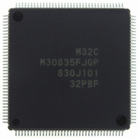
Manufacturer Part Number
M30835FJGP#U5
Description
IC M32C/83 MCU FLASH 144LQFP
Manufacturer
Renesas Electronics America
Series
M16C™ M32C/80r
Datasheets
1.M3087BFLGPU3.pdf
(364 pages)
2.M30833FJGPU3.pdf
(96 pages)
3.M30833FJGPU3.pdf
(529 pages)
Specifications of M30835FJGP#U5
Core Processor
M32C/80
Core Size
16/32-Bit
Speed
32MHz
Connectivity
CAN, I²C, IEBus, SIO, UART/USART
Peripherals
DMA, WDT
Number Of I /o
121
Program Memory Size
512KB (512K x 8)
Program Memory Type
FLASH
Ram Size
31K x 8
Voltage - Supply (vcc/vdd)
3 V ~ 5.5 V
Data Converters
A/D 34x10b, D/A 2x8b
Oscillator Type
Internal
Operating Temperature
-20°C ~ 85°C
Package / Case
144-LQFP
For Use With
R0K330879S001BE - KIT DEV RSK M32C/87R0K330879S000BE - KIT DEV RSK M32C/87
Lead Free Status / RoHS Status
Lead free / RoHS Compliant
Eeprom Size
-
Available stocks
Company
Part Number
Manufacturer
Quantity
Price

Part Number:
M30835FJGP#U5M30835FJGP#U3
Manufacturer:
Renesas Electronics America
Quantity:
10 000


R
R
M
e
E
3
. v
J
Figure 25.5 How to Enter and Exit CPU Rewrite Mode
2
0
25.3.4 How to Enter and Exit CPU Rewrite Mode
1
9
C
3 .
B
Figure 25.5 shows how to enter and exit CPU rewrite mode.
No program in the flash memory can be executed in CPU rewrite mode. Execute rewrite control program
in a space other than the flash memory (internal RAM, etc.) after transferring the program to that space.
8 /
0
1
3
0
3
J
G
4
a
0 -
n
o r
3 .
1
u
, 1
3
NOTES:
p
1
2
(
1. Set the MCD register to the following CPU clock frequency:
2. Exit CPU rewrite mode after excuting the read array command or resetting the flash memory.
3. When CPU rewrite mode is exited while the FMR05 bit is set to "1", the user ROM area can be accessed.
M
0
Jump to the rewrite control program
transferred to space other than the flash
memory. (On the following steps, use the
rewrite control program in space other than
the flash memory.)
0
When the PM12 bit in the PM1 register is set to "0" (no internal access wait), 6.25 MHz or less
When the PM12 bit in the PM1 register is set to "1" (internal access wait), 12.5 MHz or less
3
6
Transfer the rewrite control program in
CPU rewrite mode to space other than
the flash memory
2
Set the PM0, PM1 and MCD register
C
Page 399
8 /
Single-chip mode,
Memory expansion mode,
Boot mode
, 3
M
3
2
C
f o
8 /
4
3
8
) T
8
(1)
Rewrite control program
Set the FMR01 bit to "0" (CPU rewrite mode
disabled)
In boot mode only
In boot mode only
Set the FMR03 bit to "0" after executing a
read array command or after setting the
FMR03 bit to "1"
Set the FMR05 bit to "1" (User ROM area
accessed)
Set the FMR05 bit to "0" (boot ROM area
accessed)
Set the FMR01 bit to "1" (CPU rewrite
mode enabled) following "0"
Jump to a desired address in the
flash memory
Execute software commands
(3)
(2)
25. Flash Memory Version
Related parts for M30835FJGP#U5
Image
Part Number
Description
Manufacturer
Datasheet
Request
R

Part Number:
Description:
KIT STARTER FOR M16C/29
Manufacturer:
Renesas Electronics America
Datasheet:

Part Number:
Description:
KIT STARTER FOR R8C/2D
Manufacturer:
Renesas Electronics America
Datasheet:

Part Number:
Description:
R0K33062P STARTER KIT
Manufacturer:
Renesas Electronics America
Datasheet:

Part Number:
Description:
KIT STARTER FOR R8C/23 E8A
Manufacturer:
Renesas Electronics America
Datasheet:

Part Number:
Description:
KIT STARTER FOR R8C/25
Manufacturer:
Renesas Electronics America
Datasheet:

Part Number:
Description:
KIT STARTER H8S2456 SHARPE DSPLY
Manufacturer:
Renesas Electronics America
Datasheet:

Part Number:
Description:
KIT STARTER FOR R8C38C
Manufacturer:
Renesas Electronics America
Datasheet:

Part Number:
Description:
KIT STARTER FOR R8C35C
Manufacturer:
Renesas Electronics America
Datasheet:

Part Number:
Description:
KIT STARTER FOR R8CL3AC+LCD APPS
Manufacturer:
Renesas Electronics America
Datasheet:
Part Number:
Description:
KIT STARTER FOR RX610
Manufacturer:
Renesas Electronics America
Datasheet:

Part Number:
Description:
KIT STARTER FOR R32C/118
Manufacturer:
Renesas Electronics America
Datasheet:

Part Number:
Description:
KIT DEV RSK-R8C/26-29
Manufacturer:
Renesas Electronics America
Datasheet:

Part Number:
Description:
KIT STARTER FOR SH7124
Manufacturer:
Renesas Electronics America
Datasheet:

Part Number:
Description:
KIT STARTER FOR H8SX/1622
Manufacturer:
Renesas Electronics America
Datasheet:

Part Number:
Description:
KIT DEV FOR SH7203
Manufacturer:
Renesas Electronics America
Datasheet: