M30835FJGP#U5 Renesas Electronics America, M30835FJGP#U5 Datasheet - Page 422
M30835FJGP#U5
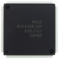
Manufacturer Part Number
M30835FJGP#U5
Description
IC M32C/83 MCU FLASH 144LQFP
Manufacturer
Renesas Electronics America
Series
M16C™ M32C/80r
Datasheets
1.M3087BFLGPU3.pdf
(364 pages)
2.M30833FJGPU3.pdf
(96 pages)
3.M30833FJGPU3.pdf
(529 pages)
Specifications of M30835FJGP#U5
Core Processor
M32C/80
Core Size
16/32-Bit
Speed
32MHz
Connectivity
CAN, I²C, IEBus, SIO, UART/USART
Peripherals
DMA, WDT
Number Of I /o
121
Program Memory Size
512KB (512K x 8)
Program Memory Type
FLASH
Ram Size
31K x 8
Voltage - Supply (vcc/vdd)
3 V ~ 5.5 V
Data Converters
A/D 34x10b, D/A 2x8b
Oscillator Type
Internal
Operating Temperature
-20°C ~ 85°C
Package / Case
144-LQFP
For Use With
R0K330879S001BE - KIT DEV RSK M32C/87R0K330879S000BE - KIT DEV RSK M32C/87
Lead Free Status / RoHS Status
Lead free / RoHS Compliant
Eeprom Size
-
Available stocks
Company
Part Number
Manufacturer
Quantity
Price

Part Number:
M30835FJGP#U5M30835FJGP#U3
Manufacturer:
Renesas Electronics America
Quantity:
10 000


R
R
M
e
E
3
. v
J
Table 25.4 Status Register
2
0
D
25.3.2 Status Register
1
9
C
7
3 .
B
The write state machine (WSM) in the flash memory controls programming and erasing of the flash
memory. The status register indicates whether or not the WSM is operating as expected, and whether or
not a program or erase operation is completed as expected. Refer to 25.3.6 Full Status Check for
details on each error.
Table 25.4 lists the status register.
The status register can be read by the read status command (Refer to 25.3.5 Software Command).
8 /
to D
0
1
25.3.2.1 Block Status After Program (SR3)
25.3.2.2 Program Status (SR4)
25.3.2.3 Erase Status (SR5)
25.3.2.4 Write State Machine (WSM) Status (SR7)
3
0
SR0 (D
SR1 (D
SR2 (D
SR3 (D
SR4 (D
SR5 (D
SR6 (D
SR7 (D
Symbol
The SR3 bit is set to "1" when a page program command execution is completed with an excessive
write error. The SR3 bit is set to "0" when the clear status command is executed.
The SR3 bit is set to "0" after reset or after setting the FMR03 bit to "0" following "1".
The SR4 bit is set to "1" when a program error occurs while the page program or lock bit program
command is being executed. The SR4 bit is set to "0" when the clear status command is executed.
The SR4 bit is set to "0" after reset or after setting the FMR03 bit to "0" following "1".
The SR5 bit is set to "1" when an erase error occurs while the block erase or erase all unlocked block
command is being executed. The SR5 bit is set to "0" when the clear status command is executed.
The SR5 bit is set to "0" after reset or after setting the FMR03 bit to "0" following "1".
The SR7 bit indicates the WSM operation state. The SR7 bit is set to "0" during auto write or auto
erase and to "1" when an auto write or auto erase operation is completed. The SR7 bit changes while
the page program, block erase, erase all unlocked block or lock bit program command is being ex-
ecuted. The SR7 bit changes with the above commands only. The SR7 bit is set to "1" after reset or
after setting the FMR03 bit to "0" following "1",.
The FMR00 bit indicates the WSM status. Read the FMR00 bit to determine whether the auto write or
erase operation is completed.
3
J
0
G
4
a
: These data bus are read when the read status register command is executed.
0 -
n
o r
3 .
1
u
0
1
2
3
4
5
6
7
, 1
3
p
)
)
)
)
)
)
)
)
1
2
(
M
0
0
3
6
2
C
Page 397
8 /
, 3
Program status
Erase status
Write state machine (WSM) status
Reserved bit
Reserved bit
Reserved bit
Block status after program
Reserved bit
M
3
2
C
f o
8 /
4
3
8
Status Name
) T
8
BUSY
-
-
-
Completed as expected
Completed as expected
Completed as expected
-
0
Definition
Error (program error)
Error (erase error)
-
-
-
Error (excessive write error)
-
READY
25. Flash Memory Version
1
Related parts for M30835FJGP#U5
Image
Part Number
Description
Manufacturer
Datasheet
Request
R

Part Number:
Description:
KIT STARTER FOR M16C/29
Manufacturer:
Renesas Electronics America
Datasheet:

Part Number:
Description:
KIT STARTER FOR R8C/2D
Manufacturer:
Renesas Electronics America
Datasheet:

Part Number:
Description:
R0K33062P STARTER KIT
Manufacturer:
Renesas Electronics America
Datasheet:

Part Number:
Description:
KIT STARTER FOR R8C/23 E8A
Manufacturer:
Renesas Electronics America
Datasheet:

Part Number:
Description:
KIT STARTER FOR R8C/25
Manufacturer:
Renesas Electronics America
Datasheet:

Part Number:
Description:
KIT STARTER H8S2456 SHARPE DSPLY
Manufacturer:
Renesas Electronics America
Datasheet:

Part Number:
Description:
KIT STARTER FOR R8C38C
Manufacturer:
Renesas Electronics America
Datasheet:

Part Number:
Description:
KIT STARTER FOR R8C35C
Manufacturer:
Renesas Electronics America
Datasheet:

Part Number:
Description:
KIT STARTER FOR R8CL3AC+LCD APPS
Manufacturer:
Renesas Electronics America
Datasheet:
Part Number:
Description:
KIT STARTER FOR RX610
Manufacturer:
Renesas Electronics America
Datasheet:

Part Number:
Description:
KIT STARTER FOR R32C/118
Manufacturer:
Renesas Electronics America
Datasheet:

Part Number:
Description:
KIT DEV RSK-R8C/26-29
Manufacturer:
Renesas Electronics America
Datasheet:

Part Number:
Description:
KIT STARTER FOR SH7124
Manufacturer:
Renesas Electronics America
Datasheet:

Part Number:
Description:
KIT STARTER FOR H8SX/1622
Manufacturer:
Renesas Electronics America
Datasheet:

Part Number:
Description:
KIT DEV FOR SH7203
Manufacturer:
Renesas Electronics America
Datasheet: