M30835FJGP#U5 Renesas Electronics America, M30835FJGP#U5 Datasheet - Page 71
M30835FJGP#U5
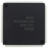
Manufacturer Part Number
M30835FJGP#U5
Description
IC M32C/83 MCU FLASH 144LQFP
Manufacturer
Renesas Electronics America
Series
M16C™ M32C/80r
Datasheets
1.M3087BFLGPU3.pdf
(364 pages)
2.M30833FJGPU3.pdf
(96 pages)
3.M30833FJGPU3.pdf
(529 pages)
Specifications of M30835FJGP#U5
Core Processor
M32C/80
Core Size
16/32-Bit
Speed
32MHz
Connectivity
CAN, I²C, IEBus, SIO, UART/USART
Peripherals
DMA, WDT
Number Of I /o
121
Program Memory Size
512KB (512K x 8)
Program Memory Type
FLASH
Ram Size
31K x 8
Voltage - Supply (vcc/vdd)
3 V ~ 5.5 V
Data Converters
A/D 34x10b, D/A 2x8b
Oscillator Type
Internal
Operating Temperature
-20°C ~ 85°C
Package / Case
144-LQFP
For Use With
R0K330879S001BE - KIT DEV RSK M32C/87R0K330879S000BE - KIT DEV RSK M32C/87
Lead Free Status / RoHS Status
Lead free / RoHS Compliant
Eeprom Size
-
Available stocks
Company
Part Number
Manufacturer
Quantity
Price

Part Number:
M30835FJGP#U5M30835FJGP#U3
Manufacturer:
Renesas Electronics America
Quantity:
10 000


R
R
M
5.2 Software Reset
5.3 Watchdog Timer Reset
e
E
3
. v
J
Table 5.1 Pin States while RESET Pin is Held "L"
2
0
NOTES:
P5
P0
P1
P2, P3, P4
P6 to P15
P5
P5
P5
P5
P5
P5
P5
When the PM03 bit in the PM0 register is set to "1" (microcomputer reset), pins, the CPU and SFR are
reset. Then the microcomputer executes the program from an address determined by the reset vector.
When software reset is performed, some registers in the SFR are not reset. Refer to 4. SFR for details.
Set the PM03 bit to "1" while the main clock is selected as the CPU clock and the main clock oscillation is
stable.
The microcomputer resets pins, the CPU and the SFR when the watchdog timer underflows while the
CM06 bit in the CM0 register is set to "1" (reset). Then the microcomputer executes the program from an
address indicated by the reset vector.
When watchdog timer reset is performed, some registers in the SFR are not reset. Refer to 4. SFR for
details. Because the PM01 to PM00 bits in the PM0 register are not reset, the processor mode remains
unchanged.
Pin Name
1
9
C
3 .
B
1. Ports P11 to P15 are provided in the 144-pin package.
8 /
4
0
1
2
3
5
6
7
0
1
3
0
3
J
G
4
a
0 -
n
o r
3 .
(1)
1
u
3
, 1
p
1
2
(
M
0
0
3
6
2
C
8 /
Page 46
Input port (high-impedance)
CNV
Input port (high-impedance)
Input port (high-impedance)
Input port (high-impedance)
Input port (high-impedance)
Input port (high-impedance)
Input port (high-impedance)
Input port (high-impedance)
Input port (high-impedance)
Input port (high-impedance)
Input port (high-impedance)
Input port (high-impedance)
, 3
M
SS
3
2
____________
= V
C
f o
8 /
SS
4
3
8
) T
8
CNV
HLDA output (output value depends on an input to HOLD pin)
BYTE = V
Data input (high-impedance)
Data input (high-impedance)
BHE output (indeterminate)
BCLK output
HOLD input (high-impedance)
RAS output
Input port (high-impedance)
Address output (indeterminate)
WR output (output "H")
RDY input (high-impedance)
RD output (output "H")
SS
= V
SS
CC
Pin States
Input port (high-impedance)
BYTE = V
CC
5. Reset
Related parts for M30835FJGP#U5
Image
Part Number
Description
Manufacturer
Datasheet
Request
R

Part Number:
Description:
KIT STARTER FOR M16C/29
Manufacturer:
Renesas Electronics America
Datasheet:

Part Number:
Description:
KIT STARTER FOR R8C/2D
Manufacturer:
Renesas Electronics America
Datasheet:

Part Number:
Description:
R0K33062P STARTER KIT
Manufacturer:
Renesas Electronics America
Datasheet:

Part Number:
Description:
KIT STARTER FOR R8C/23 E8A
Manufacturer:
Renesas Electronics America
Datasheet:

Part Number:
Description:
KIT STARTER FOR R8C/25
Manufacturer:
Renesas Electronics America
Datasheet:

Part Number:
Description:
KIT STARTER H8S2456 SHARPE DSPLY
Manufacturer:
Renesas Electronics America
Datasheet:

Part Number:
Description:
KIT STARTER FOR R8C38C
Manufacturer:
Renesas Electronics America
Datasheet:

Part Number:
Description:
KIT STARTER FOR R8C35C
Manufacturer:
Renesas Electronics America
Datasheet:

Part Number:
Description:
KIT STARTER FOR R8CL3AC+LCD APPS
Manufacturer:
Renesas Electronics America
Datasheet:
Part Number:
Description:
KIT STARTER FOR RX610
Manufacturer:
Renesas Electronics America
Datasheet:

Part Number:
Description:
KIT STARTER FOR R32C/118
Manufacturer:
Renesas Electronics America
Datasheet:

Part Number:
Description:
KIT DEV RSK-R8C/26-29
Manufacturer:
Renesas Electronics America
Datasheet:

Part Number:
Description:
KIT STARTER FOR SH7124
Manufacturer:
Renesas Electronics America
Datasheet:

Part Number:
Description:
KIT STARTER FOR H8SX/1622
Manufacturer:
Renesas Electronics America
Datasheet:

Part Number:
Description:
KIT DEV FOR SH7203
Manufacturer:
Renesas Electronics America
Datasheet: