M30835FJGP#U5 Renesas Electronics America, M30835FJGP#U5 Datasheet - Page 83
M30835FJGP#U5
Manufacturer Part Number
M30835FJGP#U5
Description
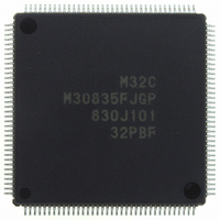
IC M32C/83 MCU FLASH 144LQFP
Manufacturer
Renesas Electronics America
Series
M16C™ M32C/80r
Datasheets
1.M3087BFLGPU3.pdf
(364 pages)
2.M30833FJGPU3.pdf
(96 pages)
3.M30833FJGPU3.pdf
(529 pages)
Specifications of M30835FJGP#U5
Core Processor
M32C/80
Core Size
16/32-Bit
Speed
32MHz
Connectivity
CAN, I²C, IEBus, SIO, UART/USART
Peripherals
DMA, WDT
Number Of I /o
121
Program Memory Size
512KB (512K x 8)
Program Memory Type
FLASH
Ram Size
31K x 8
Voltage - Supply (vcc/vdd)
3 V ~ 5.5 V
Data Converters
A/D 34x10b, D/A 2x8b
Oscillator Type
Internal
Operating Temperature
-20°C ~ 85°C
Package / Case
144-LQFP
For Use With
R0K330879S001BE - KIT DEV RSK M32C/87R0K330879S000BE - KIT DEV RSK M32C/87
Lead Free Status / RoHS Status
Lead free / RoHS Compliant
Eeprom Size
-
Available stocks
Company
Part Number
Manufacturer
Quantity
Price

Part Number:
M30835FJGP#U5M30835FJGP#U3
Manufacturer:
Renesas Electronics America
Quantity:
10 000


R
R
M
e
E
3
. v
J
2
Figure 7.3 WCR Register
0
7.2.4 Bus Timing
C
1
9
3 .
B
8 /
Bus cycle for the internal ROM and internal RAM are basically one BCLK cycle. When the PM12 bit in the
PM1 register is set to "1" (wait state), the bus cycles are two BCLK cycles.
Bus cycles for the SFR are basically two BCLK cycles. When the PM13 bit in the PM1 register is set to "1"
(2 wait states), the bus cycles are three BCLK cycles. To access CAN-associated registers (addresses
01E0
Bus cycle for an external space is basically one BCLK cycle for a read operation and two BCLK cycles for
a write operation. The WCR register inserts wait states equivalent to one to three BCLK cycles into an
external space. Bus cycles are two BCLK cycles if selecting one wait state. Bus cycles are four BCLK
cycles if selecting three wait states.
If applicable to the followings, bus cycles vary from those selected by the WCR register. Figure 7.5
shows each bit status and bus cycle.
Figure 7.3 shows the WCR register. Figures 7.4 and 7.5 show bus timing in an external space.
0
1
3
0
• Write cycle with the separate bus and no wait state
• Read cycle and write cycle with the multiplexed bus and no wait state.
• Read cycle and write cycle with the multiplexed bus and one wait state.
3
J
G
4
a
16
o r
Wait Control Register
0 -
n
b7
3 .
1
u
to 0245
, 1
3
p
b6
NOTES:
1
(
2
M
b5
1. When using the multiplexed bus, "2 waits" is selected even if the WCR register is set to "00
2. When using the separate bus, the read bus runs one BCLK cycle and the write bus runs two
0
3.The WCR register cannot be used in M32C/83T.
0
3
wait state) or "01
BCLK cycles (1 wait state) if the WCR register is set to "00
6
2
b4
16
C
8 /
), set the PM13 bit to "1".
b3
Page 58
, 3
b2
M
b1
3
2
C
b0
f o
2
8 /
" (1 wait state). "10
4
3
Symbol
8
WCR0
WCR1
WCR2
WCR3
WCR4
WCR5
WCR6
WCR7
) T
8
Bit
(1, 2, 3)
Symbol
WCR
External Space 0
Wait Bit
External Space 1
Wait Bit
External Space 2
Wait Bit
External Space 3
Wait Bit
Bit Name
2
" (2 wait states) and "11
Address
0008
16
b1 b0
b3 b2
b5 b4
b7 b6
0 0: No wait state
0 1: 1 wait state
1 0: 2 wait states
1 1: 3 wait states
0 0: No wait state
0 1: 1 wait state
1 0: 2 wait states
1 1: 3 wait states
0 0: No wait state
0 1: 1 wait state
1 0: 2 wait states
1 1: 3 wait states
0 0: No wait state
0 1: 1 wait state
1 0: 2 wait states
1 1: 3 wait states
2
".
2
" (3 wait states) can be selected.
After Reset
1111 1111
Function
2
2
" (no
RW
RW
RW
RW
RW
RW
RW
RW
RW
7. Bus
Related parts for M30835FJGP#U5
Image
Part Number
Description
Manufacturer
Datasheet
Request
R

Part Number:
Description:
KIT STARTER FOR M16C/29
Manufacturer:
Renesas Electronics America
Datasheet:

Part Number:
Description:
KIT STARTER FOR R8C/2D
Manufacturer:
Renesas Electronics America
Datasheet:

Part Number:
Description:
R0K33062P STARTER KIT
Manufacturer:
Renesas Electronics America
Datasheet:

Part Number:
Description:
KIT STARTER FOR R8C/23 E8A
Manufacturer:
Renesas Electronics America
Datasheet:

Part Number:
Description:
KIT STARTER FOR R8C/25
Manufacturer:
Renesas Electronics America
Datasheet:

Part Number:
Description:
KIT STARTER H8S2456 SHARPE DSPLY
Manufacturer:
Renesas Electronics America
Datasheet:

Part Number:
Description:
KIT STARTER FOR R8C38C
Manufacturer:
Renesas Electronics America
Datasheet:

Part Number:
Description:
KIT STARTER FOR R8C35C
Manufacturer:
Renesas Electronics America
Datasheet:

Part Number:
Description:
KIT STARTER FOR R8CL3AC+LCD APPS
Manufacturer:
Renesas Electronics America
Datasheet:
Part Number:
Description:
KIT STARTER FOR RX610
Manufacturer:
Renesas Electronics America
Datasheet:

Part Number:
Description:
KIT STARTER FOR R32C/118
Manufacturer:
Renesas Electronics America
Datasheet:

Part Number:
Description:
KIT DEV RSK-R8C/26-29
Manufacturer:
Renesas Electronics America
Datasheet:

Part Number:
Description:
KIT STARTER FOR SH7124
Manufacturer:
Renesas Electronics America
Datasheet:

Part Number:
Description:
KIT STARTER FOR H8SX/1622
Manufacturer:
Renesas Electronics America
Datasheet:

Part Number:
Description:
KIT DEV FOR SH7203
Manufacturer:
Renesas Electronics America
Datasheet: