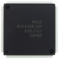
M30835FJGP#U5 Renesas Electronics America, M30835FJGP#U5 Datasheet - Page 327

M30835FJGP#U5
Manufacturer Part Number
M30835FJGP#U5
Description
IC M32C/83 MCU FLASH 144LQFP
Manufacturer
Renesas Electronics America
Series
M16C™ M32C/80r
Datasheets
1.M3087BFLGPU3.pdf
(364 pages)
2.M30833FJGPU3.pdf
(96 pages)
3.M30833FJGPU3.pdf
(529 pages)
Specifications of M30835FJGP#U5
Core Processor
M32C/80
Core Size
16/32-Bit
Speed
32MHz
Connectivity
CAN, I²C, IEBus, SIO, UART/USART
Peripherals
DMA, WDT
Number Of I /o
121
Program Memory Size
512KB (512K x 8)
Program Memory Type
FLASH
Ram Size
31K x 8
Voltage - Supply (vcc/vdd)
3 V ~ 5.5 V
Data Converters
A/D 34x10b, D/A 2x8b
Oscillator Type
Internal
Operating Temperature
-20°C ~ 85°C
Package / Case
144-LQFP
For Use With
R0K330879S001BE - KIT DEV RSK M32C/87R0K330879S000BE - KIT DEV RSK M32C/87
Lead Free Status / RoHS Status
Lead free / RoHS Compliant
Eeprom Size
-
Available stocks
Company
Part Number
Manufacturer
Quantity
Price
Part Number:
M30835FJGP#U5M30835FJGP#U3
Manufacturer:
Renesas Electronics America
Quantity:
10 000
- Current page: 327 of 529
- Download datasheet (5Mb)
R
R
M
e
E
3
. v
J
2
Figure 21.40 Transmit Operation
Figure 21.41 Receive Operation
9 0
. 1
C
Transfer clock
SIOiTR bit
The above applies under the following conditions:
Transfer clock
ISTxDi pin
TI bit
TXEPT bit
B
1 3
8 /
• The STPS bit in the GiMR register is set to "0" (1 stop bit)
• The UFORM bit in the GiMR register is set to "0" (LSB first)
• The INV bits in the GiPOCR0 to GiPOCR7 registers are set to "0" (no inverse)
• The IRS bit in the GiMR register is set to "0" (no data in the transmit buffer)
0
The above applies under the following conditions:
ISRxDi pin
RI bit
SIOiRR bit
3
3 0
• The STPS bit in the GiMR register is set to "0" (1 stop bit)
• The UFORM bit in the GiMR register is set to "0" (LSB first)
• The INV bits in the GiPOCR0 to GiPOCR7 registers are set to "0" (no inverse)
J
G
- 4
n a
o r
1 0
3 .
u
, 1
1 3
p
0 2
(
M
"H"
"L"
"1"
"0"
"1"
"0"
6 0
3
"H"
"L"
"1"
"0"
"1"
"0"
"1"
"0"
2
C
8 /
Page 302
, 3
M
3
2
ST
C
f o
Set data in the GiTB register
ST
8 /
D
0
4
3
8 8
D
D
) T
1
0
D
D
2
1
D
D
3
2
D
D
4
3
D
Tc
D
5
4
D
D
Write "0" by program
if setting to "0"
6
5
D
D
7
6
SP
21. Intelligent I/O (Group 0, 1 Communication Function)
D
7
SP
Write "0" by program
if setting to "0"
ST
i : 0,1
SIOiRR bit : Bit in the IIOkIR register (k = 0,2)
RI bit
i : 0,1
TI, TXEPT bit : Bits in the GiCR register
SIOiTR bit
Read the GiDRB register
D
0
Set data in the GiTB register
ST
D
1
D
: Bit in the GiCR register
D
0
2
: Bit in the IIOjIR register (j = 1,3)
D
D
1
3
D
D
2
4
D
D
3
5
D
D
4
6
D
D
5
7
SP
D
6
D
7
SP
Related parts for M30835FJGP#U5
Image
Part Number
Description
Manufacturer
Datasheet
Request
R

Part Number:
Description:
KIT STARTER FOR M16C/29
Manufacturer:
Renesas Electronics America
Datasheet:

Part Number:
Description:
KIT STARTER FOR R8C/2D
Manufacturer:
Renesas Electronics America
Datasheet:

Part Number:
Description:
R0K33062P STARTER KIT
Manufacturer:
Renesas Electronics America
Datasheet:

Part Number:
Description:
KIT STARTER FOR R8C/23 E8A
Manufacturer:
Renesas Electronics America
Datasheet:

Part Number:
Description:
KIT STARTER FOR R8C/25
Manufacturer:
Renesas Electronics America
Datasheet:

Part Number:
Description:
KIT STARTER H8S2456 SHARPE DSPLY
Manufacturer:
Renesas Electronics America
Datasheet:

Part Number:
Description:
KIT STARTER FOR R8C38C
Manufacturer:
Renesas Electronics America
Datasheet:

Part Number:
Description:
KIT STARTER FOR R8C35C
Manufacturer:
Renesas Electronics America
Datasheet:

Part Number:
Description:
KIT STARTER FOR R8CL3AC+LCD APPS
Manufacturer:
Renesas Electronics America
Datasheet:

Part Number:
Description:
KIT STARTER FOR RX610
Manufacturer:
Renesas Electronics America
Datasheet:

Part Number:
Description:
KIT STARTER FOR R32C/118
Manufacturer:
Renesas Electronics America
Datasheet:

Part Number:
Description:
KIT DEV RSK-R8C/26-29
Manufacturer:
Renesas Electronics America
Datasheet:

Part Number:
Description:
KIT STARTER FOR SH7124
Manufacturer:
Renesas Electronics America
Datasheet:

Part Number:
Description:
KIT STARTER FOR H8SX/1622
Manufacturer:
Renesas Electronics America
Datasheet:

Part Number:
Description:
KIT DEV FOR SH7203
Manufacturer:
Renesas Electronics America
Datasheet:


