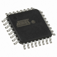
AT90LS2333-4AI Atmel, AT90LS2333-4AI Datasheet - Page 23

AT90LS2333-4AI
Manufacturer Part Number
AT90LS2333-4AI
Description
IC MCU 2K 4MHZ A/D LV IT 32TQFP
Manufacturer
Atmel
Series
AVR® 90LSr
Datasheet
1.AT90LS2333-4AC.pdf
(103 pages)
Specifications of AT90LS2333-4AI
Core Processor
AVR
Core Size
8-Bit
Speed
4MHz
Connectivity
SPI, UART/USART
Peripherals
Brown-out Detect/Reset, POR, PWM, WDT
Number Of I /o
20
Program Memory Size
2KB (1K x 16)
Program Memory Type
FLASH
Eeprom Size
128 x 8
Ram Size
128 x 8
Voltage - Supply (vcc/vdd)
2.7 V ~ 6 V
Data Converters
A/D 6x10b
Oscillator Type
Internal
Operating Temperature
-40°C ~ 85°C
Package / Case
32-TQFP, 32-VQFP
Lead Free Status / RoHS Status
Contains lead / RoHS non-compliant
To make use of the reset flags to identify a reset condition, the user should read and then clear the MCUSR as early as
possible in the program. If the register is cleared before another reset occurs, the source of the reset can be found by
examining the reset flags.
Interrupt Handling
The AT90S2333/4433 has two 8-bit Interrupt Mask control registers; GIMSK - General Interrupt Mask register and TIMSK -
Timer/Counter Interrupt Mask register.
When an interrupt occurs, the Global Interrupt Enable I-bit is cleared (zero) and all interrupts are disabled. The user soft-
ware can set (one) the I-bit to enable nested interrupts. The I-bit is set (one) when a Return from Interrupt instruction - RETI
- is executed.
When the Program Counter is vectored to the actual interrupt vector in order to execute the interrupt handling routine, hard-
ware clears the corresponding flag that generated the interrupt. Some of the interrupt flags can also be cleared by writing a
logic one to the flag bit position(s) to be cleared.
If an interrupt condition occurs when the corresponding interrupt enable bit is cleared (zero), the interrupt flag will be set
and remembered until the interrupt is enabled, or the flag is cleared by software.
If one or more interrupt conditions occur when the global interrupt enable bit is cleared (zero), the corresponding interrupt
flag(s) will be set and remembered until the global interrupt enable bit is set (one), and will be executed by order of priority.
Note that external level interrupt does not have a flag, and will only be remembered for as long as the interrupt condition is
active.
Note that the status register is not automatically stored when entering an interrupt routine and restored when returning from
an interrupt routine. This must be handled by software.
General Interrupt Mask Register - GIMSK
•
When the INT1 bit is set (one) and the I-bit in the Status Register (SREG) is set (one), the external pin interrupt is enabled.
The Interrupt Sense Control1 bits 1/0 (ISC11 and ISC10) in the MCU general Control Register (MCUCR) defines whether
the external interrupt is activated on rising or falling edge of the INT1 pin or level sensed. Please note that INTF1 flag is not
set when level sensitive interrupt condition is met. However, INT1 interrupt is generated, provided that INT1 mask bit is set
in GIMSK register. Activity on the pin will cause an interrupt request even if INT1 is configured as an output. The corre-
sponding interrupt of External Interrupt Request 1 is executed from program memory address $002. See also “External
Interrupts”.
•
When the INT0 bit is set (one) and the I-bit in the Status Register (SREG) is set (one), the external pin interrupt is enabled.
The Interrupt Sense Control0 bits 1/0 (ISC01 and ISC00) in the MCU general Control Register (MCUCR) defines whether
the external interrupt is activated on rising or falling edge of the INT0 pin or level sensed. Please note that INTF0 flag is not
set when level sensitive interrupt condition is met. However, INT0 interrupt is generated, provided that INT0 mask bit is set
in GIMSK register. Activity on the pin will cause an interrupt request even if INT0 is configured as an output. The corre-
sponding interrupt of External Interrupt Request 0 is executed from program memory address $001. See also “External
Interrupts.”
•
These bits are reserved bits in the AT90S2333/4433 and always read as zero.
Bit
$3B ($5B)
Read/Write
Initial value
Bit 7 - INT1: External Interrupt Request 1 Enable
Bit 6 - INT0: External Interrupt Request 0 Enable
Bits 5..0 - Res: Reserved bits
INT1
R/W
7
0
INT0
R/W
6
0
R
5
0
-
R
4
0
-
AT90S/LS2333 and AT90S/LS4433
R
3
0
-
R
2
0
-
R
1
0
-
R
0
0
-
GIMSK
23


